Illumination apparatus, exposure apparatus using the same and device fabrication method

a technology of illumination apparatus and exposure apparatus, which is applied in the field of illumination optical systems, can solve the problems of deteriorating semiconductor wafers, lcds, thin-film magnetic heads, and the like, and achieves the effect of shortening the length of the reflection and high light utilization efficiency

Inactive Publication Date: 2005-03-15
CANON KK
View PDF28 Cites 13 Cited by
  • Summary
  • Abstract
  • Description
  • Claims
  • Application Information

AI Technical Summary

Benefits of technology

Accordingly, it is an exemplary object of the present invention to provide a small-sized illumination apparatus with high light utilization efficiency by properly shortening the length of a reflection type opt

Problems solved by technology

High-resolution patterns are unavailable without satisfactorily uniform illuminance on the illuminated plane.
However, it has not yet been verified that an illumination apparatus with a conventional reflection type optical integrator actually illuminates the illuminated plane uniformly and effectively (in other words, with desired illuminance).
Uneven illumination would cause an insufficient transfer of a pattern onto a resist, thus deteriorating quality of semiconductor wafers, LCDs, thin-film magnetic heads, and the like.
Nevertheless, the smaller s

Method used


Image

  • Illumination apparatus, exposure apparatus using the same and device fabrication method
  • Illumination apparatus, exposure apparatus using the same and device fabrication method
  • Illumination apparatus, exposure apparatus using the same and device fabrication method

Examples


Embodiment Construction

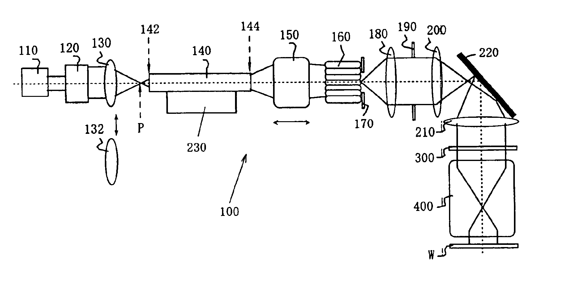
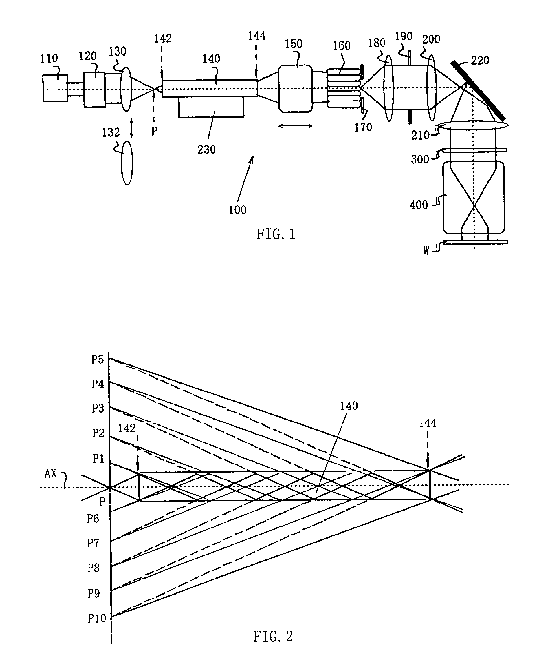
A description will now be given of an exemplary exposure apparatus 1 and illumination apparatus 100 of the present invention with reference to accompanying drawings. The same reference numeral in each figure denotes the same members. Here, FIG. 1 is a schematic block diagram of an exposure apparatus 1 and an illumination apparatus 100 of this invention that is a part of it.

As shown in FIG. 1, the exposure apparatus 1 includes the illumination apparatus 100, a mask 300, a projection optical system 400, and a controller (not shown). The exposure apparatus 1 is, for example, a scanning projection exposure apparatus that exposes onto a plate W a pattern formed on the mask 300 in a step-and-scan manner. However, the exposure apparatus of the present invention can be a step-and-repeat type exposure apparatus.

Typically, the illumination apparatus 100 includes a light source part, an illumination optical system, and a controller (not shown), thus illuminating the mask 300 on which a pattern...


PUM


Abstract

An illumination apparatus for using a beam emitted from a light source to illuminate an object area includes a condensing optical system for condensing the beam emitted from the light source, and a reflection type optical integrator located between the condensing optical system and the object area, the optical integrator having an m-gonal (where m is an even number) sectional shape, forming multiple pairs of opposing reflection surfaces, and reflecting the beam between the multiple pairs of opposing reflection surfaces, wherein a length L in an axial direction of the reflection type optical integrator meets the following equations: R=Φ/[tan {sin−1(sin θ/n)}]; and C×(A−0.1)×R≦L≦C×(A+0.1) X R, where n is a refractive index of a medium between the reflection surfaces, Φ is a distance between the reflection surfaces, θ is an angle of divergence when the beam emitted from the condensing optical system enters the reflection type optical integrator, C is a constant determined in relation to the sectional shape of the reflection type optical integrator, and A is a natural number.

Description

BACKGROUND OF THE INVENTIONThe present invention relates generally to illumination optical systems, and more particularly to an illumination apparatus, an exposure apparatus, a device fabricating method, and a device fabricated from an object to be exposed or a target. The illumination apparatuses and exposure apparatuses are used to fabricate various devices such as single crystal plates for semiconductor wafers, glass plates for liquid crystal displays (LCD), and the like. The present Invention is suitably applicable, for example, to an illumination apparatus used for an exposure apparatus that exposes single crystal plates for semiconductor wafers in a micro-lithography process for fabricating minute patterns.Along with the recent demand on smaller and lower profile electronic devices, minute semiconductor devices to be mounted onto these electronic devices have been increasingly demanded. For example, a design rule for a mask pattern requires that an image with a size of a line ...

Claims


Application Information

Patent Timeline
IPC IPC(8): G02B27/00G02F1/1335G02F1/13G02B6/42G02F1/13357
CPCG03F7/70075G02B6/4298
Inventor SHINODA, KENICHIRO
Owner CANON KK
Why Eureka
Try Eureka