Lightweight circuit board with conductive constraining cores

a technology of conductive constraining cores and circuit boards, which is applied in the direction of metallic pattern materials, synthetic resin layered products, natural mineral layered products, etc., can solve the problems of leadless chip carriers being especially susceptible to disengagement from the pwb, thermal management problems, fracture or fatigue,

Inactive Publication Date: 2005-03-22
STABLCOR TECH
View PDF13 Cites 54 Cited by
  • Summary
  • Abstract
  • Description
  • Claims
  • Application Information

AI Technical Summary

Benefits of technology

In one aspect, the invention relates to a structure and method in which a thermally conductive layer is provided in a PWB or a portion thereof. For example, the invention may include a prepreg layer made of a substitute impregnated with a resin which is thermally conductive, and possibly also electrically conductive. A laminate may be formed from such a prepreg layer, the laminate having first and second metallic layers positioned above and below the prepreg. Alternatively, the laminate may itself be thermally and / or electrically conductive, enabling its use in a high performance printed wiring board.

Problems solved by technology
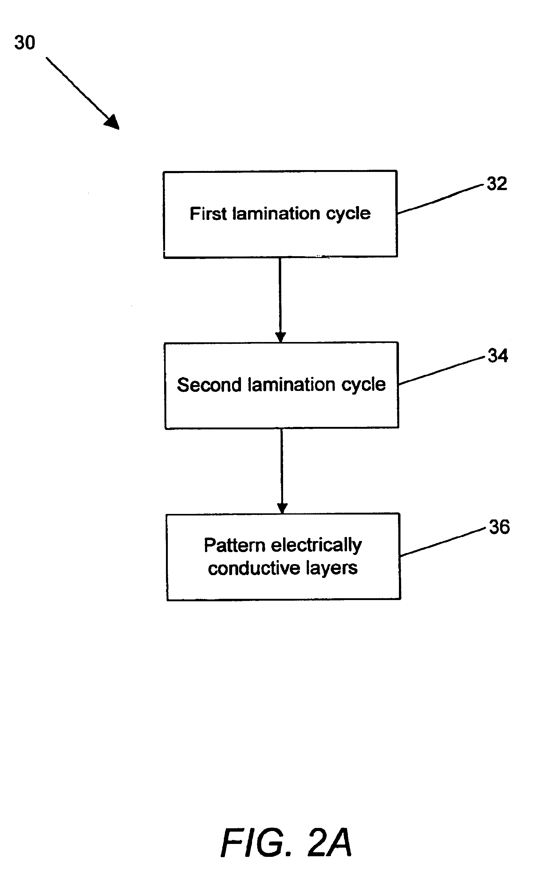
The greater density of components on the PWBs and hotter components resulted in thermal management problems.
CTE mismatch between the PWBs and components can result in fracture or fatigue during the thermal cycling caused by powering on and off of electronic devices.
Leadless chip carriers are especially susceptible to disengagement from the PWB when there are CTE mismatches.
However, these materials add undesirable weight.
The ability of previous PWBs to conduct heat away from the components mounted on their surfaces is limited by the prepreg used to prevent electrical conductivity between the functional layers of the PWB.
The materials used in prepreg have poor thermal conduction properties.
Therefore, the ability of the carbon constraining layer to conduct heat away from the surface of the board was limited by the amount of prepreg between it and the surface of the board.

Method used


Image

  • Lightweight circuit board with conductive constraining cores
  • Lightweight circuit board with conductive constraining cores
  • Lightweight circuit board with conductive constraining cores

Examples


Embodiment Construction

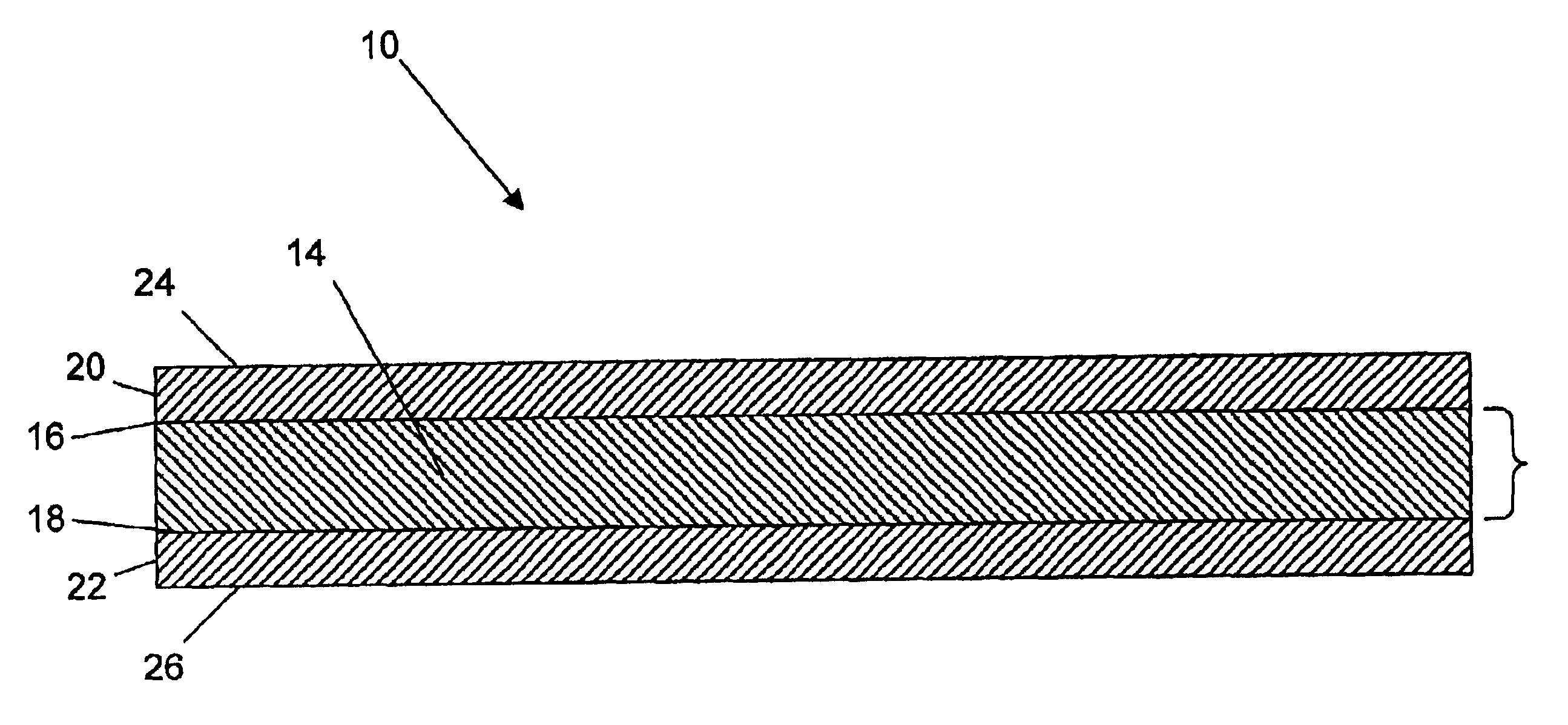
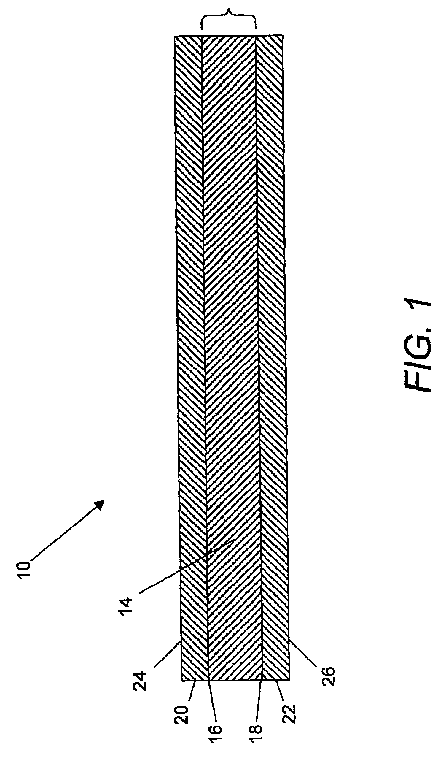
Referring now to the drawings, a printed wiring board (“PWB”) 10″″ in accordance with an embodiment of the present invention is shown in FIG. 10. The PWB includes a first laminate 120, and a second laminate 122, multiple layers of prepreg 124 and multiple layers of metal 126. The PWB 10″″ contains circuits and is used for mounting integrated circuits (ICs) and components. The term circuit is used to describe an electrically conductive path between two or more points. Individual layers of the PWB can include circuits and a number of circuits on several layers of the PWB can be connected to create an overall PWB circuit. The layers on which circuits are located are often referred to as functional layers.

The laminates 120 and 122 comprise a carbon containing layer 14 sandwiched between a first layer of metal or other electrically conductive material 16 and a second layer of metal or other electrically conductive material 18. Both of the laminates 120 and 122 are electrically conductive...


PUM

PropertyMeasurementUnit
dielectric constantaaaaaaaaaa
dielectric constantsaaaaaaaaaa
temperatureaaaaaaaaaa

Abstract

Prepregs, laminates, printed wiring board structures and processes for constructing materials and printed wiring boards that enable the construction of printed wiring boards with improved thermal properties. In one embodiment, the prepregs include substrates impregnated with electrically and thermally conductive resins. In other embodiments, the prepregs have substrate materials that include carbon. In other embodiments, the prepregs include substrates impregnated with thermally conductive resins. In other embodiments, the printed wiring board structures include electrically and thermally conductive laminates that can act as ground and / or power planes.

Description

BACKGROUND OF THE INVENTIONMultiple-layer printed circuit boards or printed wiring boards (PWBs) are used for mounting integrated circuits (ICs) and other components. The push to decrease circuit size and weight and to operate at higher frequencies and clock speeds has led to smaller components generating greater heat and being placed more closely together on the PWB. Additional size and speed improvements have also been achieved by reducing the footprints of the components by using leadless chip carriers.The greater density of components on the PWBs and hotter components resulted in thermal management problems. The Coefficient of Thermal Expansion (“CTE”) mismatch between the PWBs and the components becomes more important when greater temperatures are generated. CTE mismatch between the PWBs and components can result in fracture or fatigue during the thermal cycling caused by powering on and off of electronic devices. Leadless chip carriers are especially susceptible to disengageme...

Claims


Application Information

Patent Timeline
Patent Type & Authority Patents(United States)
IPC IPC(8): B32B27/04B32B5/26B32B5/22C08K9/00C08K9/08C08K3/38C08K3/00H05K3/46H05K1/03H05K1/02H05K3/42H05K3/44C08J5/24D03D15/275
CPCB32B5/26C08K3/38C08K9/08H05K1/0207H05K1/0366H05K1/0373H05K3/4641B32B27/04Y10T29/49124C08K2003/385H05K1/0206H05K3/429H05K3/445H05K3/4623H05K2201/0209H05K2201/0278H05K2201/0287H05K2201/0323Y10S428/901Y10T428/24917Y10T428/292Y10T29/49165Y10T428/25Y10T428/249942Y10T428/249946Y10T428/249947Y10T428/249952Y10T428/249951Y10T428/31504Y10T428/24994Y10T442/117Y10T428/249945Y10T442/2418B32B2457/00B32B2260/021B32B2307/202B32B2307/302B32B2262/101B32B2262/106B32B27/12
Inventor VASOYA, KALU K.MANGROLIA, BHARAT M.DAVIS, WILLIAM E.BOHNER, RICHARD A.
Owner STABLCOR TECH
Why Eureka
Try Eureka