Method and its apparatus for manufacturing semiconductor device

a semiconductor and manufacturing technology, applied in the direction of printers, instruments, camera focusing arrangement, etc., can solve the problems of not being able to monitor the quality of exposure light and focus using an actual product circuit pattern, so as to eliminate the need for evacuating operation, improve yield, and improve yield

Inactive Publication Date: 2005-03-22
HITACHI LTD
View PDF6 Cites 21 Cited by
  • Summary
  • Abstract
  • Description
  • Claims
  • Application Information

AI Technical Summary

Benefits of technology

With the above arrangement, since the deviations from the optimum values of the exposure light quantity and focus of the product circuit pattern can be found based on the measured data of the test pattern, the exposure light quantity and focus of a fine device having a narrow margin can be controlled at the same time with an improved yield.
As the product circuit pattern, further, a pattern having the strictest exposure light quantity and focus tolerances or margins to dimensional specifications within the exposure original plate can be selected. As a result, since optimum values are found to a pattern providing the highest yield, the yield can be improved over a yield when a product circuit pattern in another region is used.
As the signal waveform, a change in the reflected light intensity of the test pattern with respect to the wavelength or incident angle of illumination light can be used. When compared with the SEM or the like case using a signal waveform, this method can eliminate the need for evacuating operation and can increase a throughput acquired by the signal waveform. In addition, in the case of the SEM, irradiation of an electron beam may cause a change of the sectional profile of a pattern to be measured; whereas, in the case of the light irradiation, there is almost no such a danger of damage caused by such measurement.
In the first step of previously acquiring differences from the optimum values of the exposure light quantity and focus between the product circuit and test patterns within the exposure original plate, the differences from the optimum values can be calculated with use of the dimensions of the product circuit pattern and test pattern, illumination conditions at the time of light exposure, and the wave aberration of an exposure apparatus corresponding to positions of the product circuit and test patterns within the original plate. As a result, since the differences between the optimum values of the product circuit pattern and test pattern can be calculated not by experiment but by simulation, necessary data can be quickly obtained.
Further, in the second step of linking the sectional shape of the test pattern or the signal waveform associated with the sectional shape to the deviations from the optimum values of the exposure light quantity and focus and storing them as the linked information, the sectional profile of the test pattern and the signal waveform thereof can be calculated with use of the dimensions of the test pattern, illumination conditions at the time of light exposure, and the wave aberration of an exposure apparatus corresponding to a position of the test pattern within the original plate, and thus the linked information can be generated. With the above arrangement, if a plurality of exposure apparatuses are provided, then respective signal wave-form libraries (linked information) can be calculated from the wave aberrations of the exposure apparatuses, the need for performing a light exposure test for each exposure apparatus can be eliminated.

Problems solved by technology

As a result, it is impossible to monitor the quality of exposure light and focus using an actual product circuit pattern.

Method used


Image

  • Method and its apparatus for manufacturing semiconductor device
  • Method and its apparatus for manufacturing semiconductor device
  • Method and its apparatus for manufacturing semiconductor device

Examples


Embodiment Construction

Embodiments of the present invention will be detailed with reference to the attached drawings.

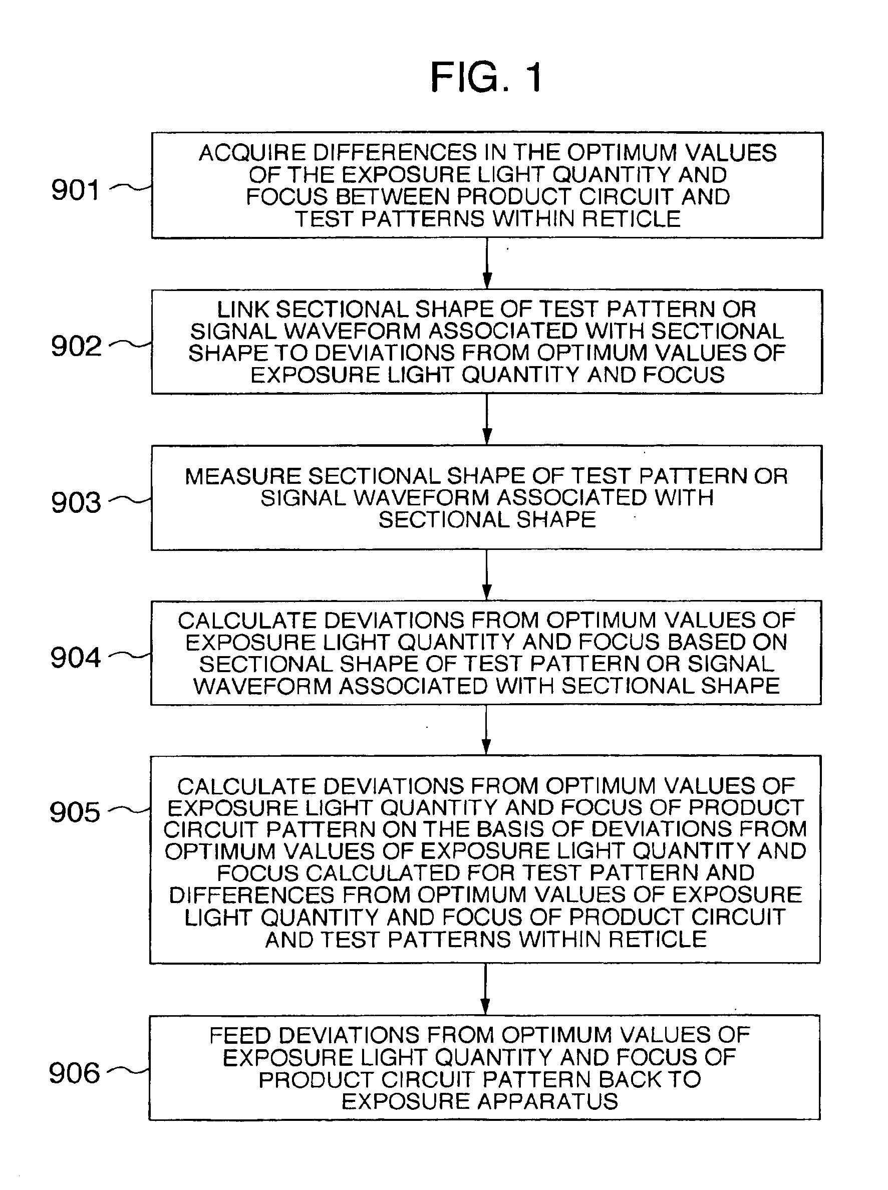
FIG. 1 is a flowchart showing an example of a method for manufacturing a semiconductor device as an embodiment of the present invention.

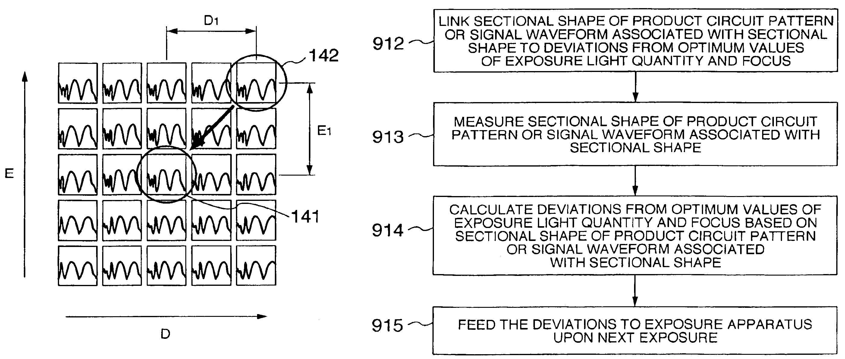
In a step 901, first of all, differences in the optimum values of the exposure light quantity and focus between a circuit pattern 51 and a test pattern 52 within a reticle 5 are previously acquired. For example, differences between the optimum values of the exposure light quantity and focus when a central dimension was specified within ±10% are given as a center offset of a process window as mentioned above. According to experimental one of methods for finding the differences, light exposure is carried out while the exposure light quantity and focus are varied to measure dimensions of transfer patterns of the circuit and test patterns 51 and 52, their process windows are plotted, and their center offsets are calculated. In this method, however, since the ex...


PUM

PropertyMeasurementUnit
reflection intensityaaaaaaaaaa
wavelengthaaaaaaaaaa
incident angleaaaaaaaaaa

Abstract

Deviations from optimum values of the exposure light quantity and focus of test and product circuit patterns are predicted from the dimensions of the patterns, illumination conditions and the wave aberration of an exposure lens. A signal waveform of scatterometry of the test pattern is linked to the deviations from the optimum values of the exposure light quantity and focus to form a library. The test pattern after exposed and developed in actual steps is collated with the signal waveform in the library measured by the scatterometry to find deviations from the optimum values of the exposure light quantity and focus of the test pattern. Deviations of the optimum values of a product circuit pattern from the deviations of the test pattern are acquired on the basis of the deviations, and the acquired deviations are fed back to subsequent exposure steps.

Description

BACKGROUND OF THE INVENTIONThe present invention relates to techniques for manufacturing a semiconductor device and more particularly, to a technique which is effectively applied to a method and its apparatuses for performing accurate control over the quantity of exposure light and focus in a light exposure step.A semiconductor device is manufactured by iteratively executing, for each layer, a step of forming a conductive or insulating film on a wafer and a lithography step of applying resist as photosensitive agent on the film, exposes and develops a circuit pattern on a reticle on the resist and then etches the film with use of the residual resist as a mask to thereby form a circuit pattern on the wafer.As a reference technique to the present invention, a light exposure step of printing a pattern on a photosensitive agent in an exposure step will be explained in connection with FIG. 19. A product circuit pattern region 50 of a reticle 5 has a circuit pattern 51 depicted thereon, a...

Claims


Application Information

Patent Timeline
Patent Type & Authority Patents(United States)
IPC IPC(8): G03F7/20G01Q30/06G01Q60/00G03B3/00G01Q70/00G02B7/04G02B7/28H01L21/027
CPCG03F7/70558G03F7/70641G03F7/70625G03F7/706
Inventor YOSHITAKE, YASUHIROTAMAKI, KENJIWATANABE, MASAHIRO
Owner HITACHI LTD
Why Eureka
Try Eureka