
Method and device for characterizing a CMOS logic cell to be produced in a technology of the partially depleted silicon-on-insulator type

a technology of silicon-on-insulator and logic cell, which is applied in the field of integrated circuits, can solve the problems of overestimation or underestimate of the performance of the structure that is produced, disadvantages of floating substrate effects, and hysteresis effect in the threshold voltage of a transistor, etc., and achieves rapid evaluation of time delays and delays

Inactive Publication Date: 2005-03-22
STMICROELECTRONICS SRL
View PDF3 Cites 4 Cited by
  • Summary
  • Abstract
  • Description
  • Claims
  • Application Information

AI Technical Summary

Benefits of technology

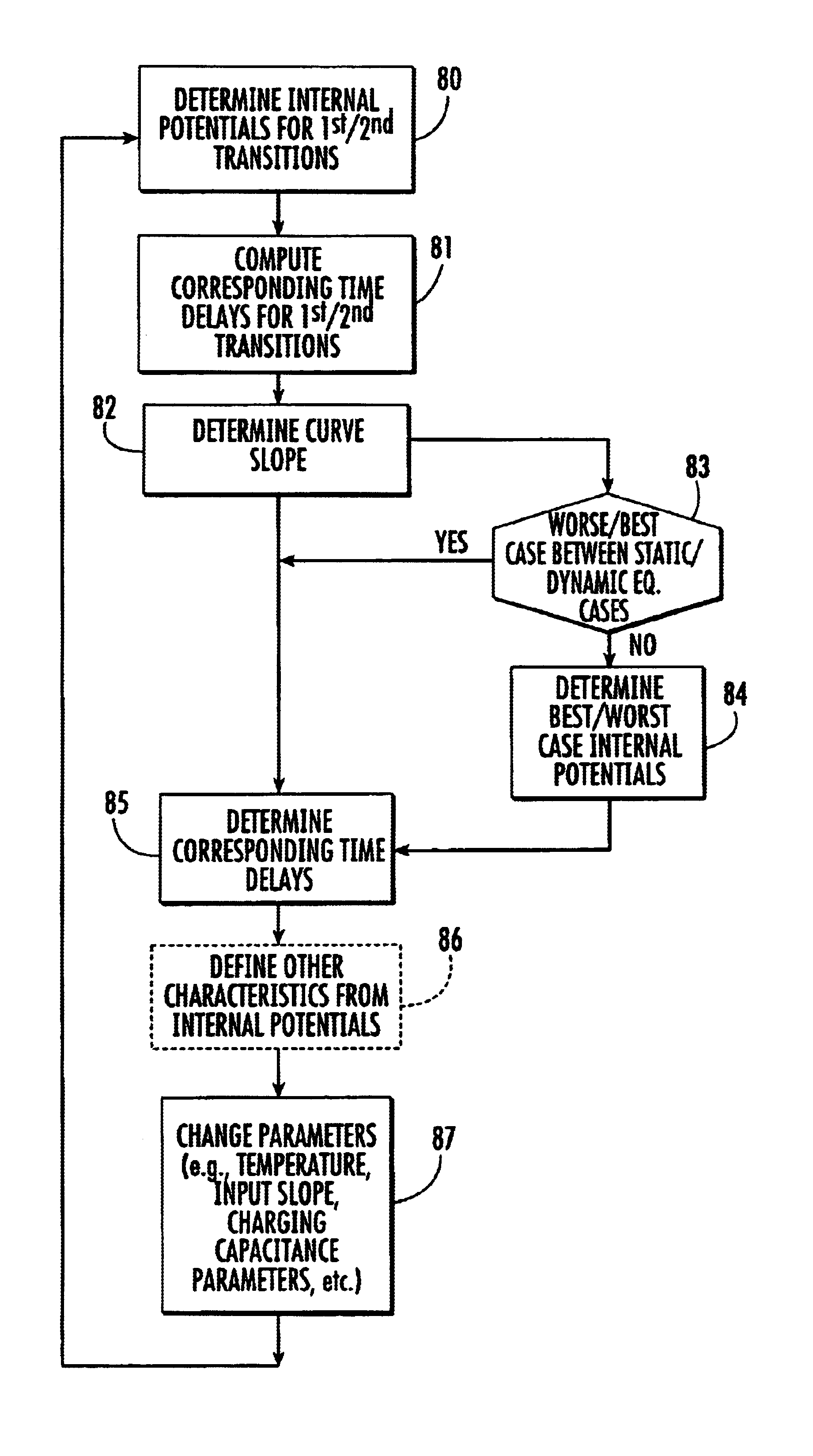
It is an object of the invention to allow rapid evaluation of time delays in a dynamic equilibrium state, as well as rapid evaluation of delays under best and worse case scenarios, for both simple and relatively complex CMOS logic cells formed using PD-SOI technology.
In other words, it is advantageous to use a parameter optimizer whose engine is, for example, a Marquardt algorithm, which is used to determine the values of the internal potentials of the transistors when the charge variation is zero between two successive transitions (i.e., the dynamic equilibrium state). As an example, the algorithm may vary n internal potentials of n transistors of the cell in question to cancel the sum of the squares of the charge variations. The parameter optimizer therefore restores the optimized values of the internal potentials of the n transistors.
It may also be advantageous to determine the internal potentials of the transistors of the cell after the first and second transitions in the stimulation signal. It may similarly be advantageous to determine the internal potentials of the transistors corresponding to the best / worse time delay cases from the internal potentials of the transistors after the first and second occurrences, and from the internal potentials in the static equilibrium state, the dynamic equilibrium state, and from the difference in rates of change.

Problems solved by technology

However, the floating substrate effects have disadvantages.
One such disadvantage is the hysteresis effect in the threshold voltage of a transistor, which is manifested by variations in time delay.
However, such an approach may result in the performance of the structure that is produced being overestimated or underestimated.
Moreover, not only do worse case delays need to be known, but the delays in the best case situations need to be known so that synchronization problems may be accounted for.
Yet, both the worse and best cases are difficult to identify since process and design parameters such as current gain, input slope, charge, supply, and temperature play a key role.
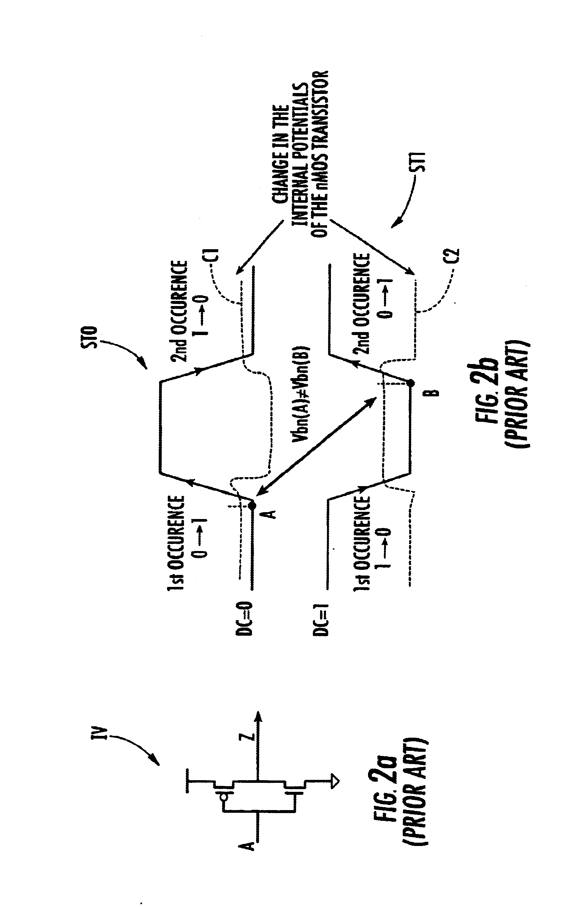
Furthermore, the variable nature of the threshold voltages in PD-SOI devices is such that the propagation of a given transition between the input and the output of a logic cell leads to a different delay depending on whether the cell is under static equilibrium (DC) conditions or whether a dynamic equilibrium (steady state AC) state has been reached.
Additionally, in practice it proves to be substantially impossible to characterize a logic cell by exhaustive simulations.
As such, the characterization of a much more complex cell is essentially inconceivable using this method.

Method used


Image

  • Method and device for characterizing a CMOS logic cell to be produced in a technology of the partially depleted silicon-on-insulator type
  • Method and device for characterizing a CMOS logic cell to be produced in a technology of the partially depleted silicon-on-insulator type
  • Method and device for characterizing a CMOS logic cell to be produced in a technology of the partially depleted silicon-on-insulator type

Examples


Embodiment Construction

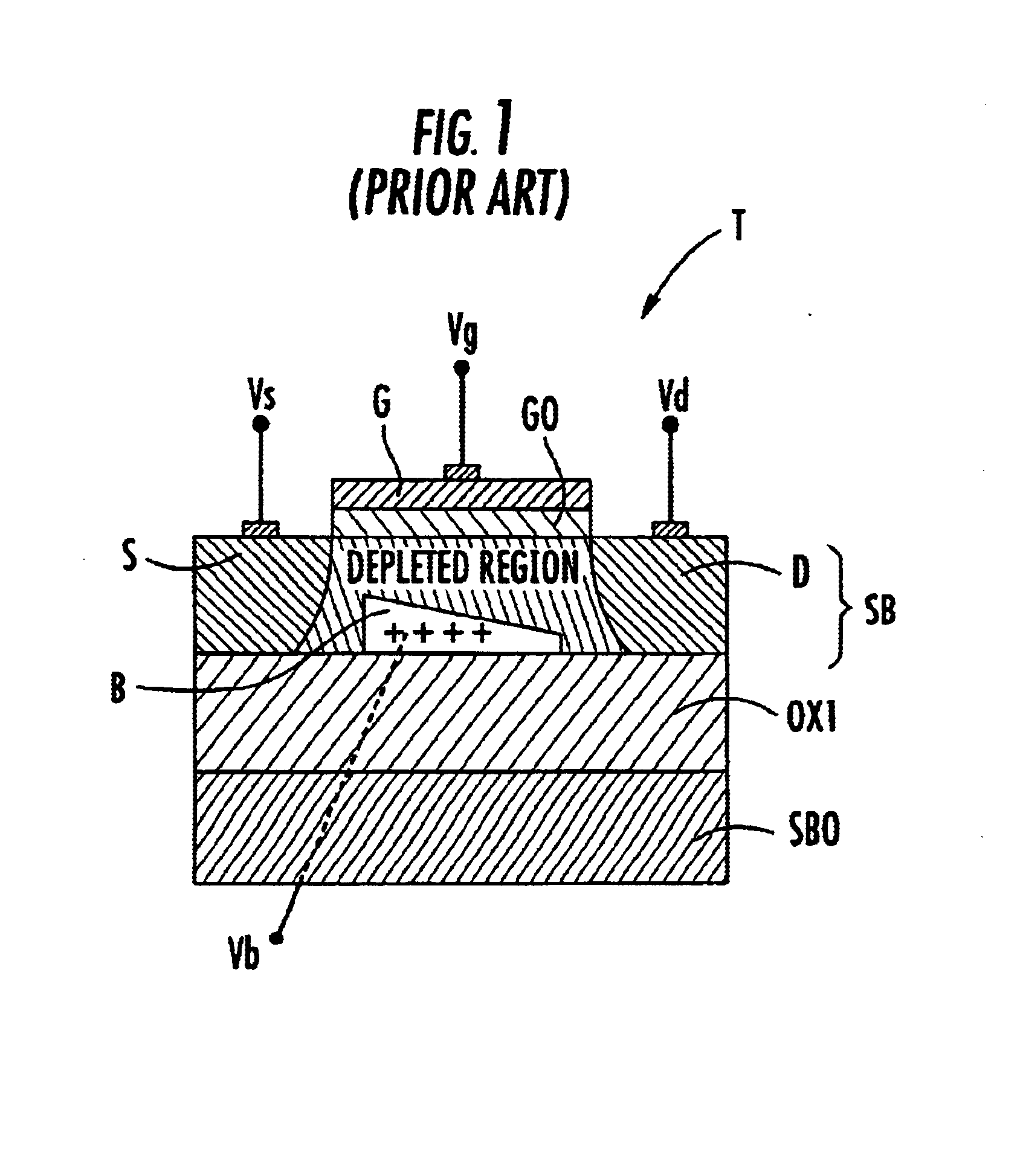
Turning now to FIG. 1, an nMOS transistor T is formed in a silicon substrate SB on an insulating layer OX1. The insulating layer OX1 itself is on a carrier substrate SBO. This structure is typical of an SOI structure, which is well known to those skilled in the art. When the thickness of the oxide layer OX1 is large enough (e.g., greater than about 50 nanometers), the substrate SB is of the partially depleted type.

In such a transistor, a neutral zone B lies beneath the depleted region and between the source and drain regions S and D. This neutral zone, which will collect holes, is not connected to a fixed potential. It is therefore referred to as a “floating substrate” zone. Of course, apart from this floating substrate zone, the transistor T conventionally includes the source region S, the drain region D and a gate region G, that latter being isolated from the substrate SB by a gate oxide GO.

The variations in the internal potential Vb of the transistor T, i.e., of the potential of ...


PUM


Abstract

A method for characterizing a CMOS logic cell of the partially depleted silicon-on-insulator type (PD-SOI) may include modeling the logic cell and determining internal potentials of transistors of the cell in a dynamic equilibrium state based upon a functional simulation of the modeled cell. This may be done using a binary stimulation signal having an initial logic value. The dynamic equilibrium state may be based upon a cancellation, to within a precision error, of the sum of the squares of variations in the quantities of charge in floating substrates of the transistors taken over a period of two successive transitions of the stimulation signal.

Description

FIELD OF THE INVENTIONThe invention relates to integrated circuits, and, more particularly, to the CMOS logic circuits. Moreover, the invention relates to the behavior of CMOS logic circuits produced using partially depleted silicon-on-insulator (PD-SOI) technology, and to the characterization of such circuits, for example, with respect to time delay.BACKGROUND OF THE INVENTIONIn recent years, SOI technology has proved to be a particularly useful alternative to conventional CMOS technology using bulk silicon. More particularly, the so-called “floating substrate” effects in SOI technology, which are well known to those skilled in the art, and the reduction in junction capacitances are two examples of the improved performance provided by SOI technology. However, the floating substrate effects have disadvantages.One such disadvantage is the hysteresis effect in the threshold voltage of a transistor, which is manifested by variations in time delay. That is, variations occur in the time ...

Claims


Application Information

Patent Timeline
Patent Type & Authority Patents(United States)
IPC IPC(8): G06F17/50
CPCG06F17/5036G06F17/5022G06F30/33G06F30/367
Inventor FLATRESSE, PHILIPPECASU, MARIO
Owner STMICROELECTRONICS SRL
Learn More