Evaluation method of semiconductor layer, method for fabricating semiconductor device, and storage medium

a semiconductor and layer technology, applied in the direction of semiconductor/solid-state device testing/measurement, optical radiation measurement, instruments, etc., can solve the problems of difficult to evaluate whether or not the implantation conditions are appropriate, measurement is considerably affected by heat treatment, and the measurement is difficult to evaluate whether or not the implantation conditions are suitable. to achieve the effect of improving the throughpu

Inactive Publication Date: 2000-10-03
PANASONIC CORP
View PDF6 Cites 67 Cited by
  • Summary
  • Abstract
  • Description
  • Claims
  • Application Information

AI Technical Summary

Benefits of technology

In accordance with this method, it is possible to determine whether the final product will be good or bad during the fabrication process of semic...

Problems solved by technology

However, when these evaluation methods are applied to the characterization during the actual fabrication process of a semiconductor device, the following problems arise.
And it has been difficult to evaluate whether or not the implantation conditions are appropriate for a region implanted with ions at a high level, in particular.
First, the RBS and the TEM are destructive test methods, and hence are not suitable for evaluation in the production line of semiconductor devices.
Furthermore, when a region implanted with a dopant at a high level is evaluated by the sheet resistance measurement, the measurement is co...

Method used


Image

  • Evaluation method of semiconductor layer, method for fabricating semiconductor device, and storage medium
  • Evaluation method of semiconductor layer, method for fabricating semiconductor device, and storage medium
  • Evaluation method of semiconductor layer, method for fabricating semiconductor device, and storage medium

Examples


embodiment 2

Next, the second embodiment, relating to the application of spectroscopic ellipsometry to the measurement of an actual temperature on a substrate surface during a process such as annealing, will be described.

Specific Example 1

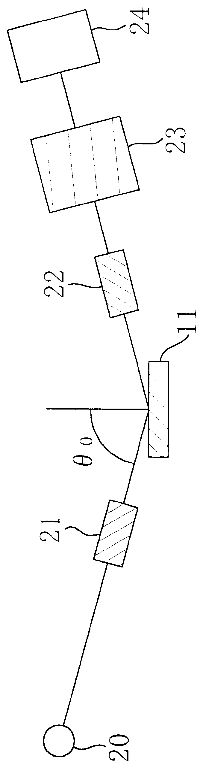
(Method for Measuring Actual Temperature on Substrate Surface)

First, the relationship between an annealing process and the thickness of an amorphous region is obtained.

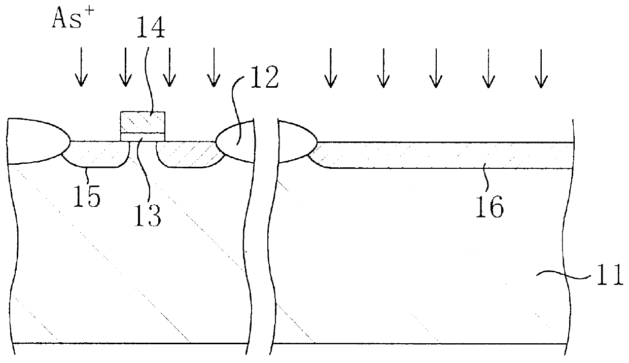
FIG. 16 shows data illustrating the relationship between the temperature at which a wafer is held and the thickness of an amorphous region where As.sup.+ ions have been implanted into the wafer at 30 keV and 3.times.10.sup.14 cm.sup.-2. The axis of abscissas indicates the power of the power supply of a degassing chamber, which is 0% in OFF State and 100% at the maximum. The degassing chamber is a chamber attached to a CVD system or a sputtering system, and a wafer is heated and retained in vacuum in the degassing chamber. The power of the degassing chamber is indicated as 0 through 100% in this m...

specific example 3

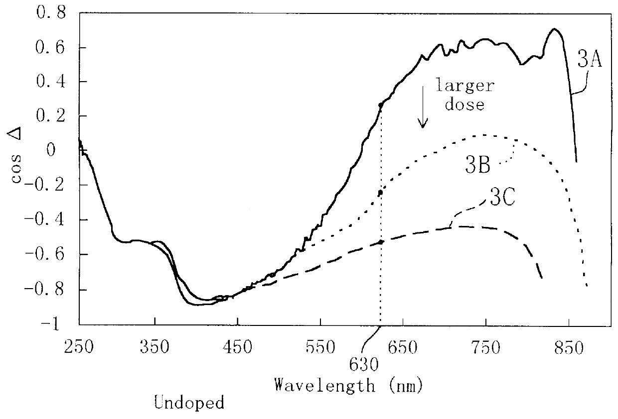
Next, a third specific example, relating to the correlation between variations in the thickness and absorption coefficient of an amorphous region (amorphous region) during annealing and a holding time obtained by measuring the thickness in accordance with the spectroscopic ellipsometry, will be described.

FIG. 18(a) shows data illustrating variations in thickness and absorption coefficient with an annealing time for various samples. In FIG. 18(a), the variation in thickness of a wafer, to which ions have been implanted at 30 keV and 4.times.10.sup.15 cm.sup.-2, is represented with .smallcircle., the variation in absorption coefficient of a wafer, to which the ions have been implanted under the same condition, is represented with .circle-solid., the variation in thickness of a wafer, to which the ions have been implanted at 30 keV and 3.times.10.sup.14 cm.sup.-2, is represented with .DELTA., and the variation in absorption coefficient of a wafer, to which the ions have been implanted ...

specific example 4

Next, a fourth specific example for finding the relationship between the annealing temperature and the variation in thickness along with the recovery of an amorphous region (amorphous region), similar to the data shown in FIG. 19, during low-temperature annealing conducted at 550.degree. C. or less, inter alia at 450.degree. C. or less, will be described.

FIG. 20(a) shows the data illustrating the dependence of a recovery rate of an amorphous region on the temperature where flash annealing has been conducted with the holding time set at substantially "0". That is to say, annealing is conducted on a wafer under a condition where the power supply is turned off immediately after the temperature has increased. The data in FIG. 20(a) is obtained in a wafer implanted with As.sup.+ ions at 30 keV and 3.times.10.sup.14 cm.sup.-2. As shown in FIG. 20(a), it can be seen that the decrease in thickness resulting from the recovery of the amorphous region varies substantially linearly with the ann...


PUM


Abstract

PCT No. PCT/JP98/02567 Sec. 371 Date Jan. 13, 1999 Sec. 102(e) Date Jan. 13, 1999 PCT Filed Jun. 10, 1998 PCT Pub. No. WO98/57146 PCT Pub. Date Dec. 17, 1998Measurement light, which has been emitted from a Xe light source (20) and then linearly polarized by a polarizer (21), is made to be incident at a tilt angle on a region in a silicon substrate (11) with crystallinity disordered by the implantation of dopant ions. And the spectra of cos DELTA and tan psi are measured with a variation of the measurement light, where DELTA is a phase difference between respective components in p and s directions as to the light reflected as an elliptically-polarized ray, and psi is a ratio between the amplitudes of these components. By correlating in advance the spectral patterns of cos DELTA and so on with the thickness of an amorphous region through a destructive test or the like, or by paying special attention to characteristic parts of the patterns of cos DELTA and so on, the thickness or the degree of disordered crystallinity of the amorphous region is estimated. Also, since a variation in the thickness of the amorphous region can be identified based on a variation of cos DELTA before and after a heat treatment, a temperature of the heat treatment can be sensed based on the variation of the thickness. Thus, an evaluation method allowing for nondestructive estimation of the thickness and the degree of disorder of a region, having crystallinity disordered by implanting dopant ions into a semiconductor region at a high level, can be provided.

Description

The present invention relates to a method for optically evaluating the characteristic of an amorphous region with crystallinity disordered by dopant ions implanted at a high level, a method for measuring a temperature and a method for fabricating a semiconductor device utilizing such evaluation, and a storage medium used for automatically making the evaluation.In a fabrication process of a semiconductor device such as a transistor, when source / drain regions for a MOSFET, an emitter diffusion layer for a bipolar transistor and so on are formed, for example, ion implantation for accelerating and implanting ions such as P, As and B into a semiconductor substrate, a polysilicon layer or an amorphous silicon film has heretofore been utilized as a means for accurately controlling doping level of the dopant, depth of a region to be doped and the like. Recently, in order to meet a demand for miniaturization of semiconductor devices, the dopant concentration and thickness of a region formed ...

Claims


Application Information

Patent Timeline
IPC IPC(8): G01N21/21H01L21/66
CPCG01N21/21H01L22/12
Inventor NANBU, YUKOSHIBATA, SATOSHI
Owner PANASONIC CORP
Why Eureka
Try Eureka