

Transfer material for wiring substrate
- Summary
- Abstract
- Description
- Claims
- Application Information
AI Technical Summary
Benefits of technology
Problems solved by technology
Method used
Image

Examples
first embodiment
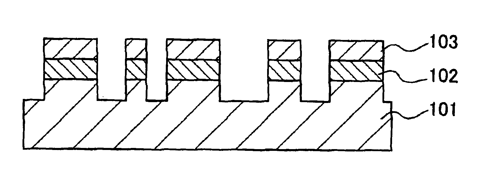
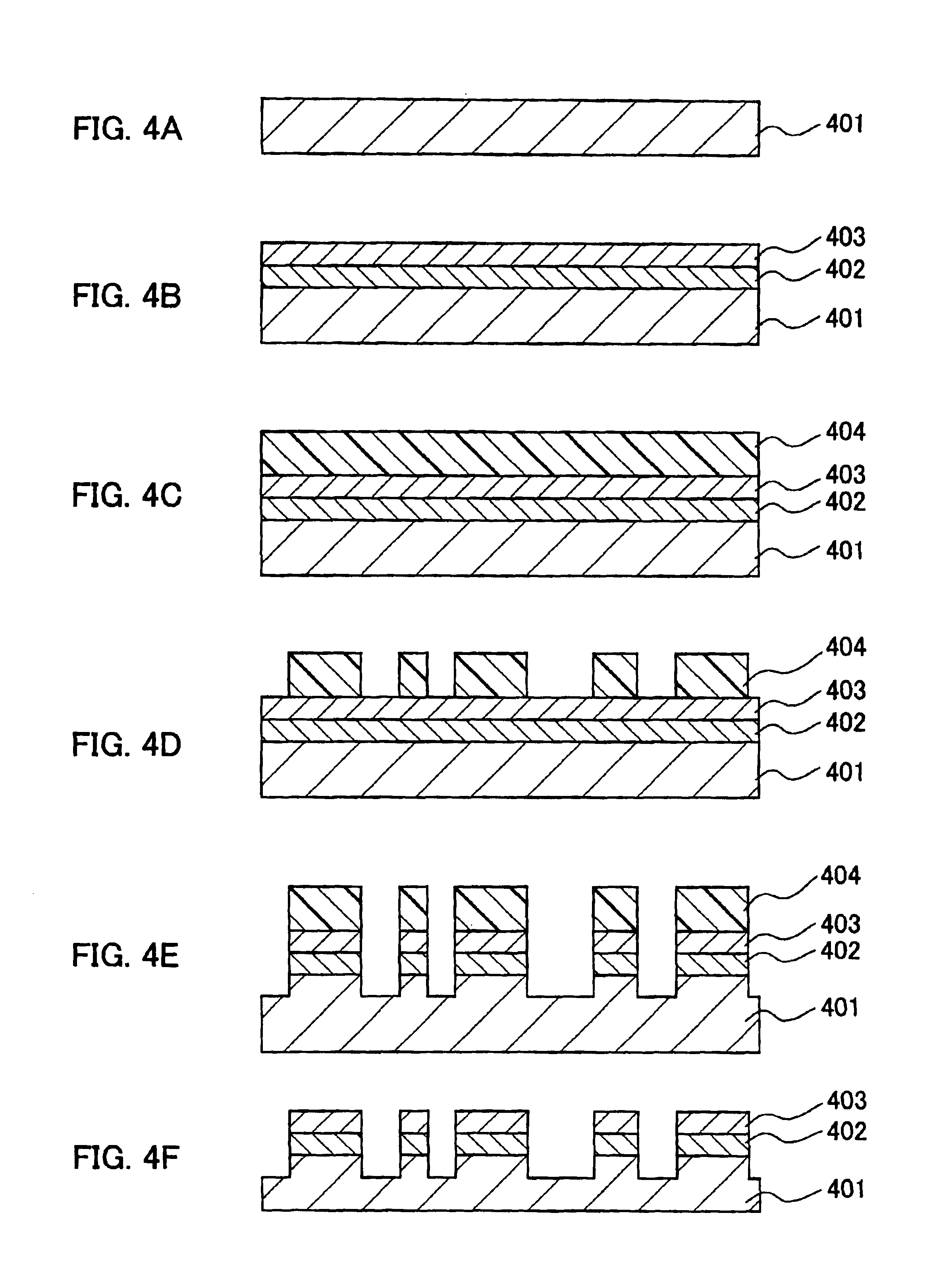
One example of a wiring pattern formation and transfer material according to a first embodiment of the present invention (hereinafter, a first transfer material will be referred to) is described. FIG. 1 is a cross-sectional view showing a schematic configuration of the first transfer material.
As shown in FIG. 1, the first transfer material includes a first metal layer 101 having a concave and convex portion (for example, the height of the convex portion is about 1 to 12 μm) on a surface portion thereof. The convex portion of the first metal layer 101 corresponds to a wiring pattern. A peel layer 102 made of an organic layer or a metal plating layer and a second metal layer 103 are formed on the convex portions. Namely, the first transfer material has a three-layered structure in which the first metal layer 101 is adhered to the second metal layer 103 with the peel layer 102 sandwiched therebetween.
In the first transfer material, the second metal layer 103 is a wiring-pattern and the...
second embodiment
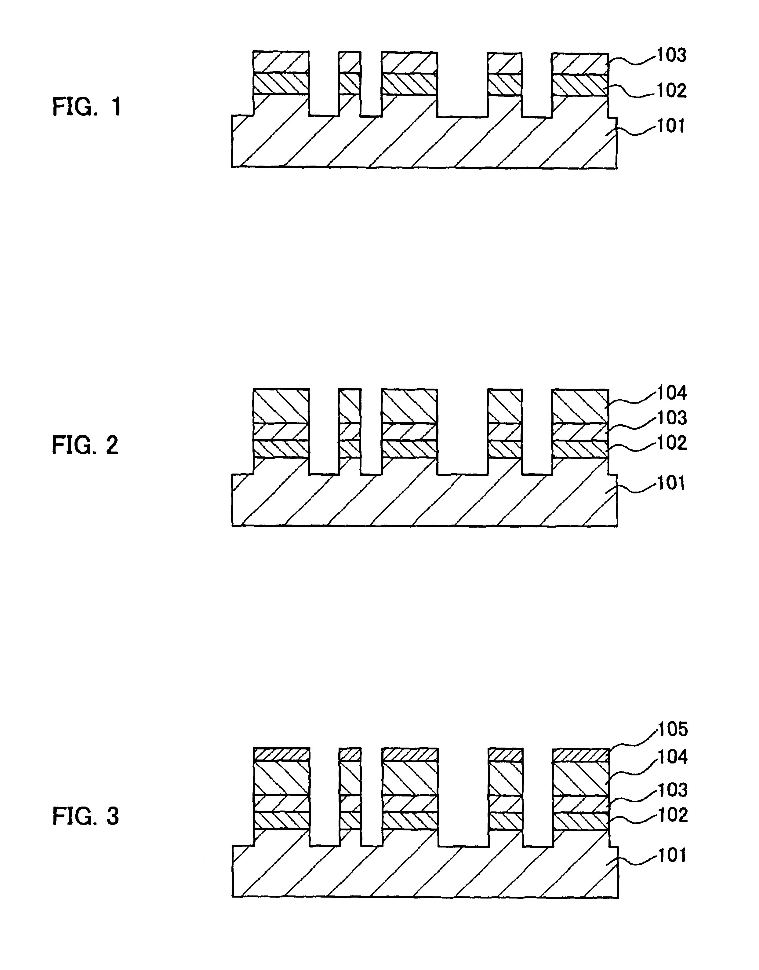
One example of a transfer material according to a second embodiment of the present invention (hereinafter, a second transfer material will be referred to) is described. FIG. 2 is a cross-sectional view showing a schematic configuration of the second transfer material.
As shown in FIG. 2, the second transfer material includes a first metal layer 101 having a concave and convex portion on a surface portion thereof. The convex portion corresponds to a wiring pattern. The second transfer material has a four-layered structure in which a peel layer 102 made of an organic layer or a metal plating layer and a second metal layer 103 are formed on the convex portion, and further a third metal layer 104 is formed on the second metal layer 103. The first metal layer 101 is adhered to the second metal layer 103 with the peel layer 102 sandwiched therebetween.
In the second transfer material, the second metal layer 103 and the third metal layer 104 make a two-layered wiring pattern and the first me...
third embodiment
One example of a transfer material according to a third embodiment of the present invention (hereinafter, a third transfer material will be referred to) is described. FIG. 3 is a cross-sectional view showing a schematic configuration of the third transfer material.
As shown in FIG. 3, the third transfer material includes a first metal layer 101 having a concave and convex portion on a surface portion thereof The convex portion corresponds to a wiring pattern. The third transfer material has a five-layered structure in which a peel layer 102 made of an organic layer or a metal plating layer and a second metal layer 103 are formed on the convex portion, further a third metal layer 104 is formed thereon, and further a fourth metal layer 105 is formed thereon. The first metal layer 101 is adhered to the second metal layer 103 via the peel layer 102.
In the third transfer material, the second metal layer 103, the third metal layer 104 and the fourth metal layer 105 make a three-layered wir...
PUM
| Property | Measurement | Unit |
|---|---|---|
| Thickness | aaaaa | aaaaa |
| Thickness | aaaaa | aaaaa |
| Thickness | aaaaa | aaaaa |
Abstract
Description
Claims
Application Information