Method for manufacturing printed wiring substrates, metal plate for use in manufacturing printed wiring substrates, and multi-printed wiring-substrate panel

Inactive Publication Date: 2005-03-29
NGK SPARK PLUG CO LTD
View PDF7 Cites 10 Cited by
  • Summary
  • Abstract
  • Description
  • Claims
  • Application Information

AI Technical Summary

Benefits of technology

The above-mentioned arrangement of the first and second depression portions involves the occurrence of those portions of the metal plate which are discontinuously located along predetermined cutting lines and at which the metal plate material is absent (i.e., the thickness of the metal

Problems solved by technology

Thus, in dicing a multi-printed wiring-substrate panel into discrete printed wiring substrates, an ordinary dicing apparatus bears a considerably heavy load and thus encounters difficulty in dicing.
If, in order to reduce the amoun

Method used


Image

  • Method for manufacturing printed wiring substrates, metal plate for use in manufacturing printed wiring substrates, and multi-printed wiring-substrate panel
  • Method for manufacturing printed wiring substrates, metal plate for use in manufacturing printed wiring substrates, and multi-printed wiring-substrate panel
  • Method for manufacturing printed wiring substrates, metal plate for use in manufacturing printed wiring substrates, and multi-printed wiring-substrate panel

Examples


Embodiment Construction

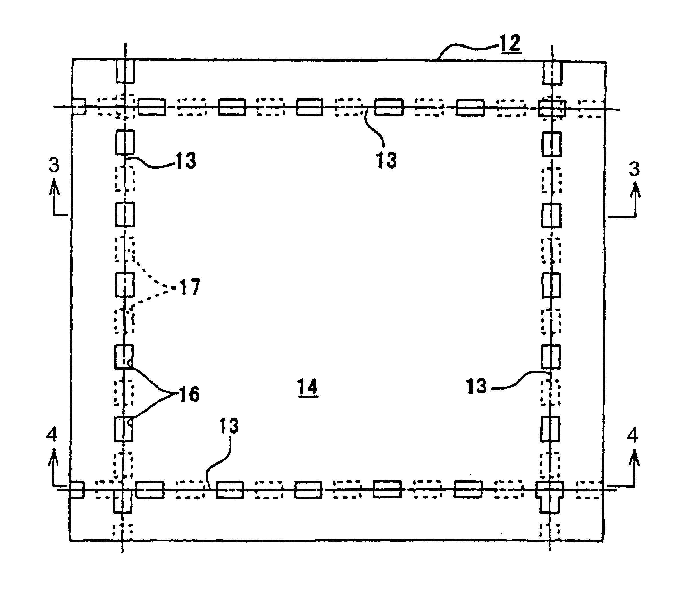
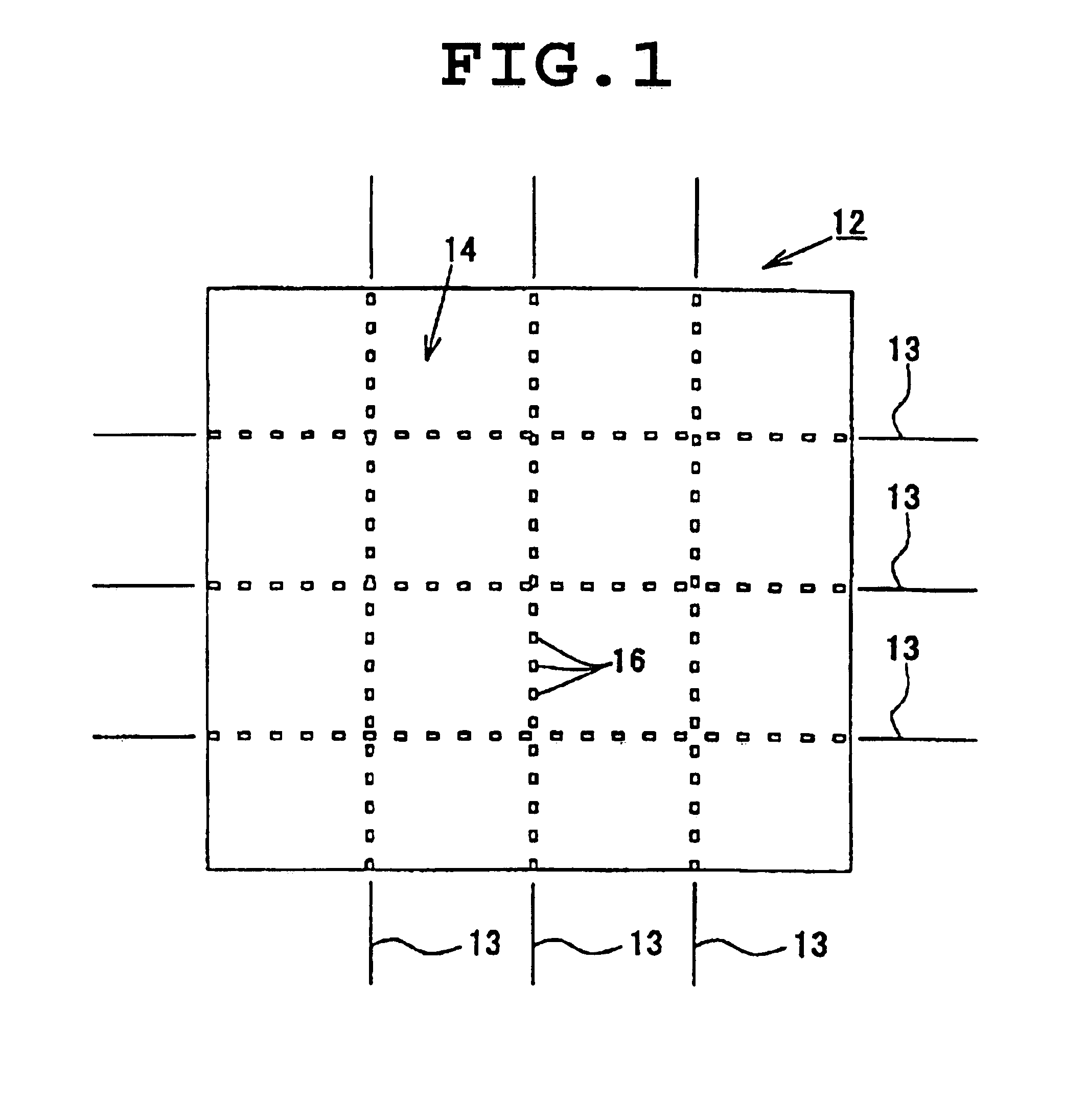
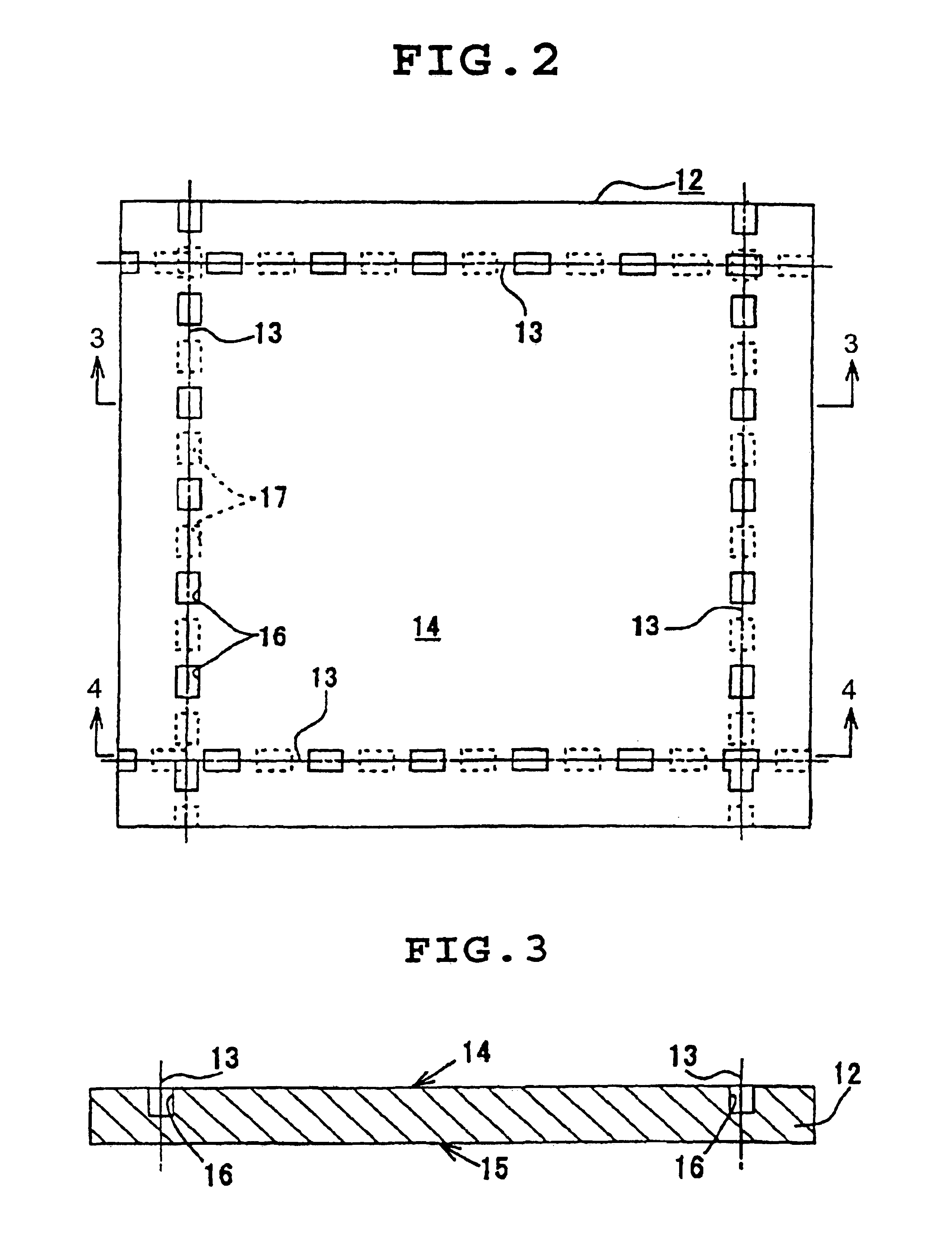
According to a conventional technique, in order to carry out dicing by use of an ordinary dicing apparatus while imposing light load on the apparatus, those portions of a metal plate (core material) which correspond to predetermined cutting lines are thinned beforehand as compared with other portions. For example, as shown in FIG. 22, continuous half-etched grooves 85 each having a width of about 0.04 inch (1 mm) are formed along latticed predetermined cutting lines 84 on one side 83 of a metal plate 82 for use in manufacturing a multi-printed wiring-substrate panel. A similar technique is also disclosed in Japanese Patent Application Laid-Open (kokai) No. 2000-133913. Cutting along the half etched grooves 85 can reduce load that is imposed on a cutting blade during the course of cutting, whereby a plurality of discrete printed wiring substrates can be obtained with relative ease.

However, the inventors of the present invention found the following: in the case where, in order to atta...


PUM

PropertyMeasurementUnit
Thicknessaaaaaaaaaa
Depthaaaaaaaaaa
Depthaaaaaaaaaa

Abstract

The invention provides a method for manufacturing printed wiring substrates which can manufacture printed wiring substrates each having resin dielectric layers of uniform thickness and excellent surface flatness while maintaining favorable cutting performance in a dicing step. A multi-printed wiring-substrate panel is manufactured which includes a metal plate having a first main surface and a second main surface, and resin dielectric layers disposed on the first and second main surfaces. The metal plate has first depression portions and second depression portions. The first depression portions are opened at the first main surface and arranged discontinuously along predetermined cutting lines. The second depression portions are opened at the second main surface and arranged discontinuously along the predetermined cutting lines. The multi-printed wiring-substrate panel is cut along the predetermined cutting lines into a plurality of printed wiring substrates.

Description

BACKGROUND OF THE INVENTION1. Field of the InventionThe present invention relates to a method for manufacturing printed wiring substrates, a metal plate for use in manufacturing printed wiring substrates, and a multi-printed wiring-substrate panel.2. Description of the Prior ArtConventionally, there is known a printed wiring substrate configured such that resin dielectric layers and wiring layers are formed on opposite sides of a metal plate, which serves as a core, or so-called metal core substrate, (refer to Japanese Patent Application Laid-Open (kokai) No. 2000-101245). A printed wiring substrate of this kind is manufactured by, for example, the following method. First, resin dielectric layers are formed on the opposite sides of the metal plate. Then, wiring layers are formed on the corresponding resin dielectric layers by means of etching or the like, thereby forming a multi-printed wiring-substrate panel, which is configured such that a plurality of printed wiring substrates ar...

Claims


Application Information

Patent Timeline
IPC IPC(8): B32B15/08B32B27/38H05K3/00H05K3/44H05K1/05
CPCB32B15/08H05K3/0052B32B27/38Y10T428/12361H05K1/056H05K3/44H05K3/445H05K2201/0909H05K2201/09709H05K2201/09745H05K2203/0369H05K2203/1572Y10S428/901Y10T428/15Y10T428/12Y10T29/49126Y10T428/24298Y10T428/24314Y10T29/49135Y10T428/24917Y10T29/49165Y10T83/0333Y10T83/0341Y10T83/0581
Inventor SUZUKI, TOMOEYURI, SHINJISATO, KAZUHISAYAMASAKI, KOZO
Owner NGK SPARK PLUG CO LTD
Why Eureka
Try Eureka