LED device and manufacturing method thereof

Inactive Publication Date: 2005-03-29
TOYODA GOSEI CO LTD +1
View PDF23 Cites 61 Cited by
  • Summary
  • Abstract
  • Description
  • Claims
  • Application Information

AI Technical Summary

Benefits of technology

Therefore, an object of the present invention is to provide an SMD type LED device in which uniformity of luminous intensity distribution characteri

Problems solved by technology

Moreover, heat-radiating characteristic is worsened compared with that of a package of a single light-emitting element.
Hence, the respective light-emitting elements become uneven both in heat-radiating characteristic and in light-emitting efficiency.
In addition, there arises a problem that color-mixing characteristic is worsened when a plurality of light-emitting element

Method used


Image

  • LED device and manufacturing method thereof
  • LED device and manufacturing method thereof
  • LED device and manufacturing method thereof

Examples


Embodiment Construction

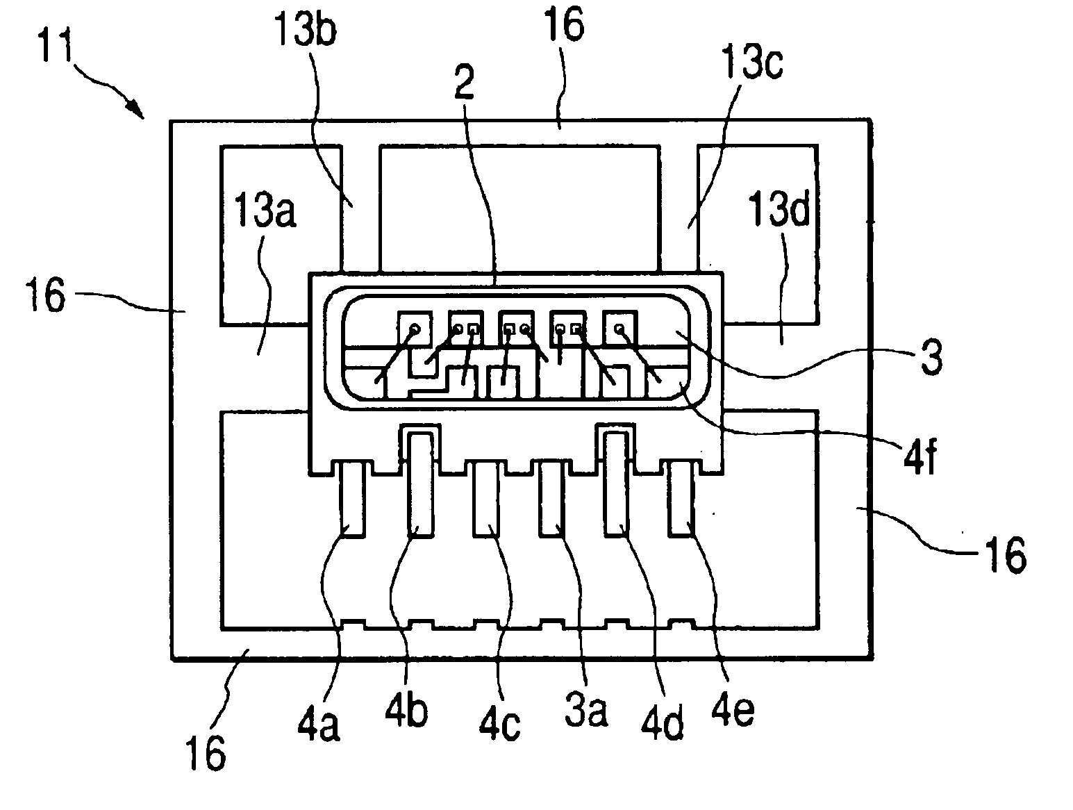
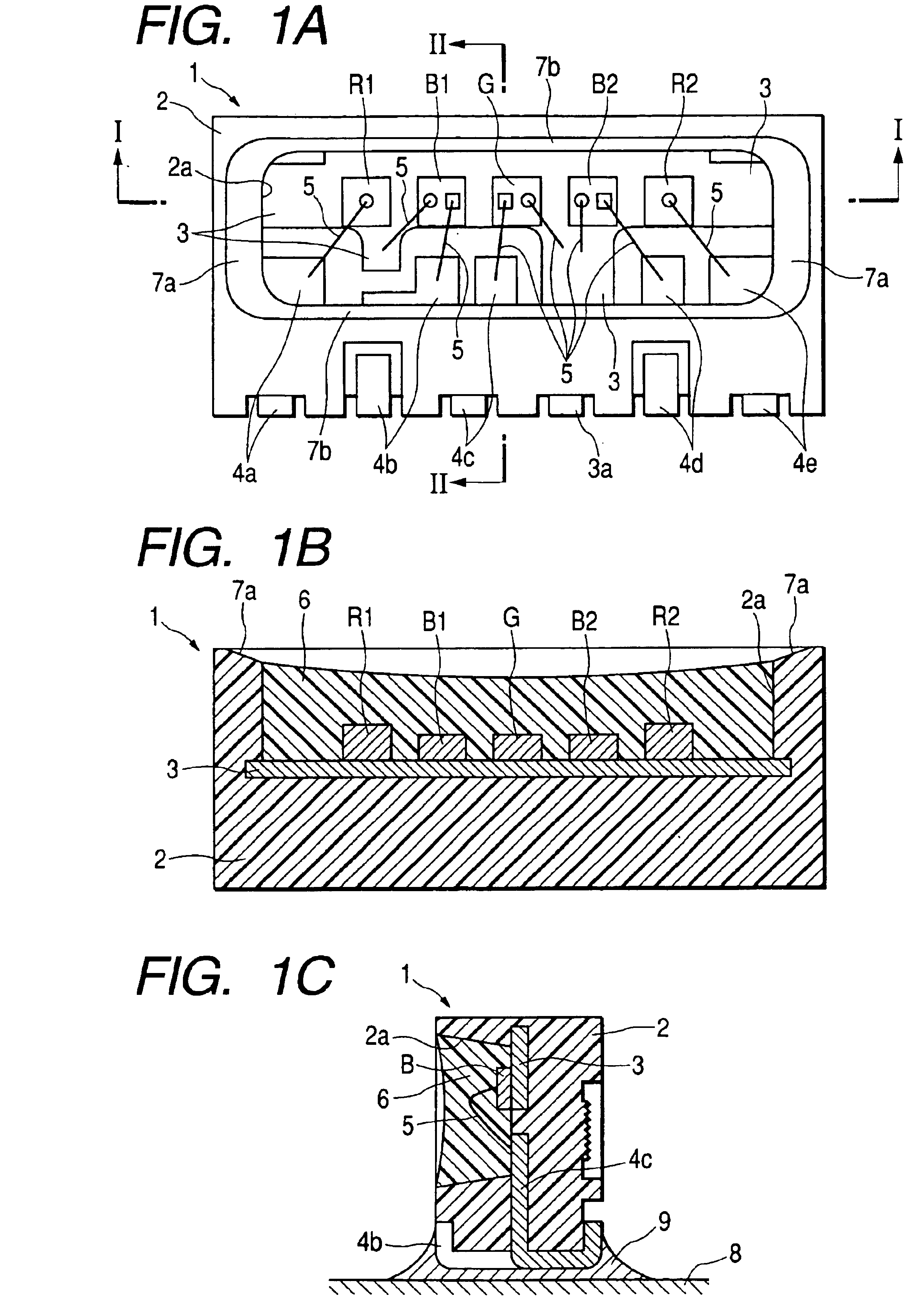
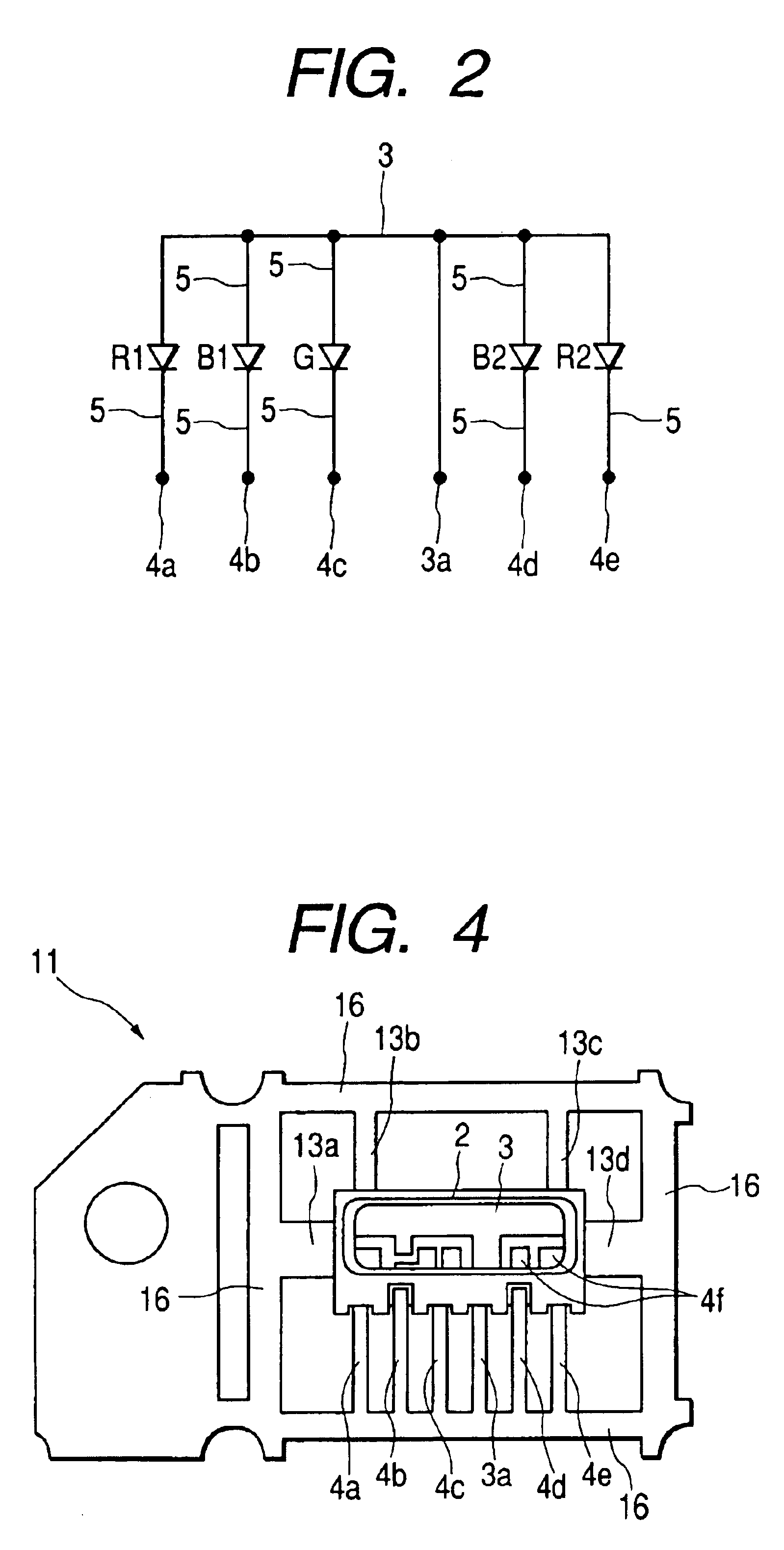
An embodiment of the invention will be described below with reference to FIGS. 1A, 1B, 1C and FIGS. 2 and 3. FIG. 1A is a front view showing the configuration of an SMD type LED lamp according to an embodiment of the LED device of the invention. FIG. 1B is a sectional view taken along the I—I in FIG. 1A. FIG. 1C is a sectional view taken along the line II—II in FIG. 1A. FIG. 2 is a circuit diagram showing the circuit configuration of the SMD type LED lamp according to the embodiment of the invention. FIG. 3 is a graph showing luminous intensity distribution characteristic of the SMD type LED lamp according to the embodiment of the invention.

As shown in FIG. 1A, in the SMD type LED lamp 1, one sheet of metal lead 3 is inserted in a synthetic resin or liquid-crystal polymer package 2 so that the lead 3 ranges from a left end or an opening portion 2a of the package 2 to a right end thereof in an upper half of the opening 2a. Two red light-emitting elements R1 and R2, two blue light-emi...


PUM


Abstract

In an LED device, an opening portion of a package in which a plurality of five light-emitting elements are mounted is filled with a transparent epoxy resin and sealed with the resin. The transparent epoxy resin is shrunk when cured. Hence, the surface of the transparent epoxy resin is dented in the center portion so that the outer edge portion becomes higher than the center portion. The light-emitting elements located at opposite ends are the highest in element height among the five light-emitting elements. Hence, when the light-emitting elements are mounted at opposite ends of a single row, distances from light-emitting surfaces of the five light-emitting elements to the surface of the transparent epoxy resin are made uniform and luminous intensity distribution characteristics thereof are made uniform. Tips of leads are further bent up along side surfaces of the package. Hence, when the LED device is soldered onto a mount board, solder is deposited even on the up-bent tips of the leads, so that surface tension of solder is balanced on the front and rear of the package. As a result, the LED device can be mounted in a predetermined position while prevented from sliding. In an LED lead frame, hanger leads are provided so as to be extended in three directions of a package. Hence, the electrically conductive leads can be bent stably and accurately without tottering of the package in the process of bending the electrically conductive leads.

Description

The present application is based on Japanese Patent Applications No. 2001-265422, 2001-265423 and 2001-265424, which are incorporated herein by reference.BACKGROUND OF THE INVENTION1. Field of the InventionThe present invention relates to a light-emitting diode lamp (hereinafter referred to as “LED lamp”) in which a single light-emitting element or a plurality of light-emitting elements, and leads and wires electrically connected to the single or plurality of light-emitting element(s) are packed in a package such as a synthetic resin package and sealed with a light-transmissive material such as a transparent epoxy resin. Incidentally, in this specification, an LED chip itself is called “light-emitting element” whereas a light-emitting device having a plurality of LED chips mounted therein is collectively called “light-emitting diode lamp” or “LED lamp”, further, more comprehensively called “LED device”. A lead frame as a raw material thereof is called “LED lead frame”.2. Description...

Claims


Application Information

Patent Timeline
IPC IPC(8): H01L25/075H01L33/00
CPCH01L25/0753H01L2224/48091H01L2224/48247H01L2224/48465H01L2924/00014H01L2924/00
Inventor MATSUMURA, KANAETAKAHASHI, YUJIKATO, HIDEAKIOHTSUKA, SHUNSUKE
Owner TOYODA GOSEI CO LTD
Why Eureka
Try Eureka