

Semiconductor device, method of manufacturing the same, and method of designing the same
a technology of semiconductor devices and semiconductors, applied in semiconductor devices, electrical devices, transistors, etc., can solve the problems of weak connection, easy thermal deformation, and weak connection portion against any physical impact,
- Summary
- Abstract
- Description
- Claims
- Application Information
AI Technical Summary
Problems solved by technology
Method used
Image

Examples
embodiment 1
This embodiment gives a description on an example in which every part of an island-like semiconductor film is on a depressive portion.
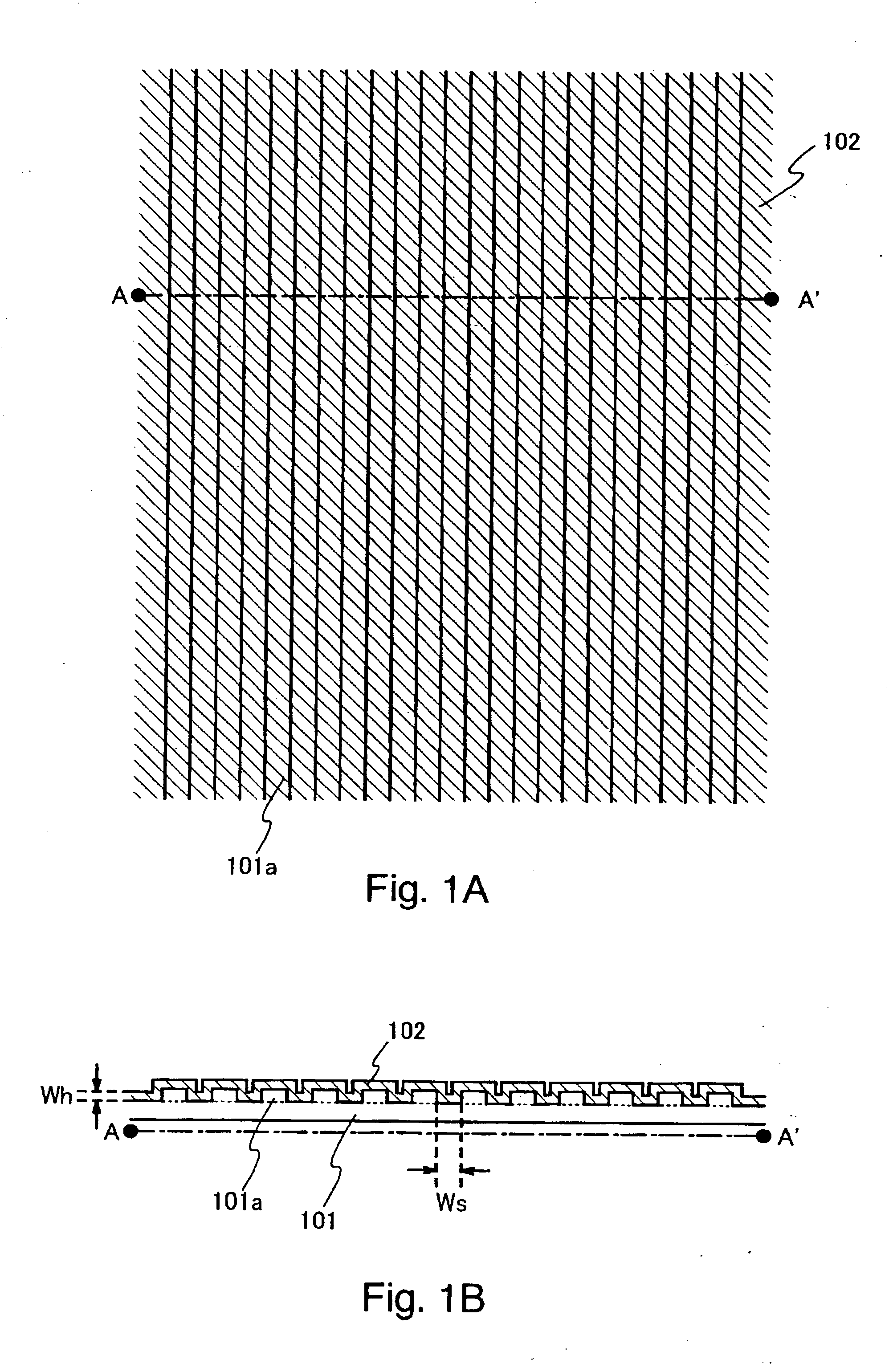
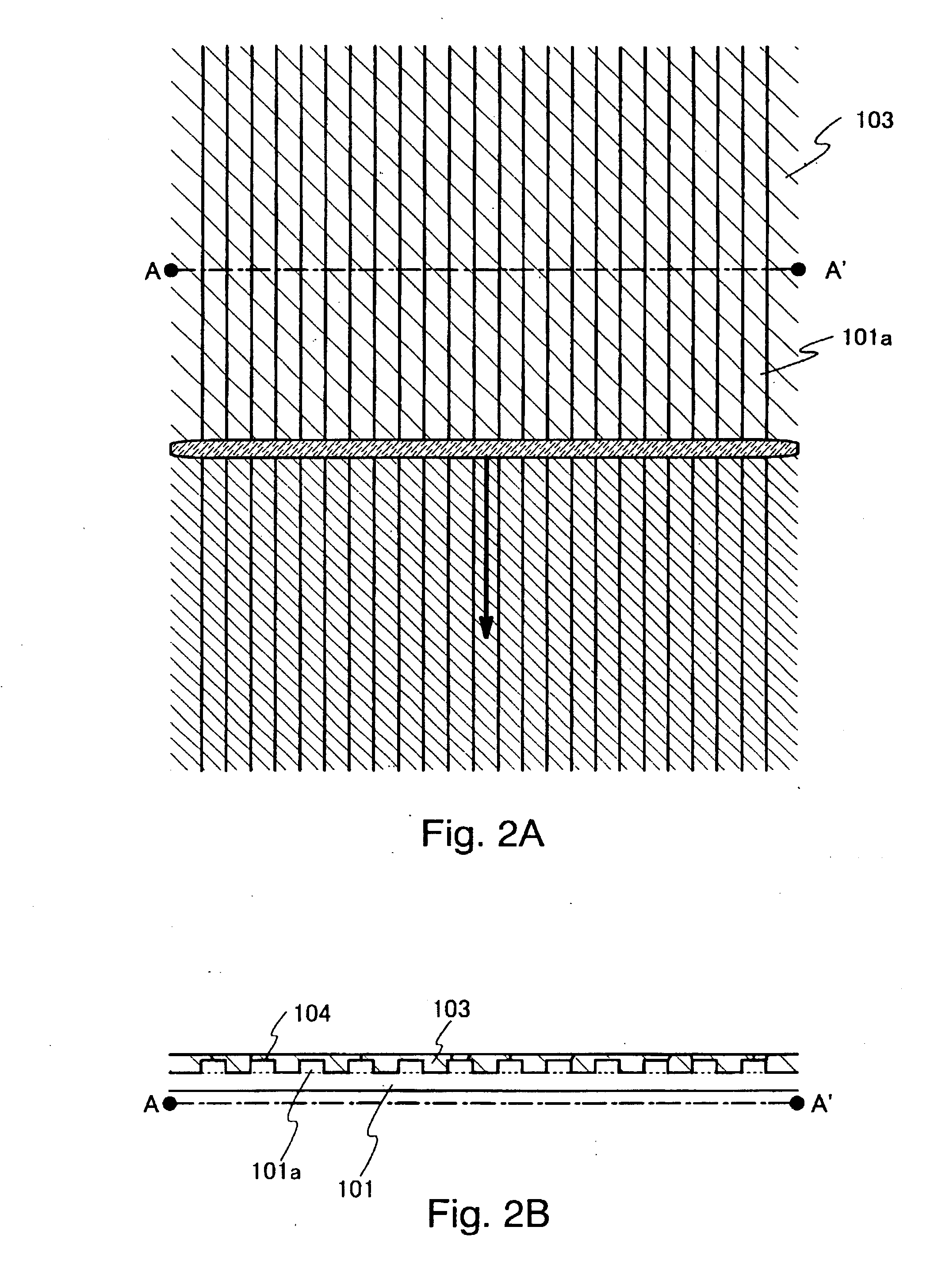
First, the state, of FIGS. 2A and 2B described in Embodiment Mode is obtained.
Next, the entire surface of the semiconductor film 103 is etched to expose the top faces of the projective portions 101a of the base film 101. Through this step, a semiconductor film is obtained which is on depressive portions alone. Any method can be used to remove the semiconductor film 103 from the top faces of the projective portions and, for example, etching or CMP is employed.
The removal from the top faces means removal of portions of the semiconductor film that are on the projective portions 101a and contain grain boundaries. As a result, a semiconductor film of excellent crystallinity is left on a depressive portion between the projective portions 101a to later serve as a channel region.
Then the semiconductor film whose surface has been etched is patterned as shown i...
embodiment 2
A method of forming a base film having unevenness is explained in Embodiment 2. Incidentally, the base film described in this embodiment is only one example and the base film used in the present invention is not limited to this structure.
A first base film 251 made from an insulating film is first formed on a substrate 250 as shown in FIG. 12A. The first base film 251 uses silicon oxynitride in this embodiment but is not limited to this material, and insulating films having a large selectivity in etching with a second base film may be used. The first base film 251 is formed by a CVD apparatus using SiH4 and N2O so that its thickness is from 50 to 200 nm. Note that the first base film may be a single layer, and may also be a laminate structure of a plurality of insulating films.
A second base film 252 is formed next from an insulating material that contacts the first base film 251, as shown in FIG. 12B. It is necessary that the film thickness of the second base film 252 be of an order ...
embodiment 3
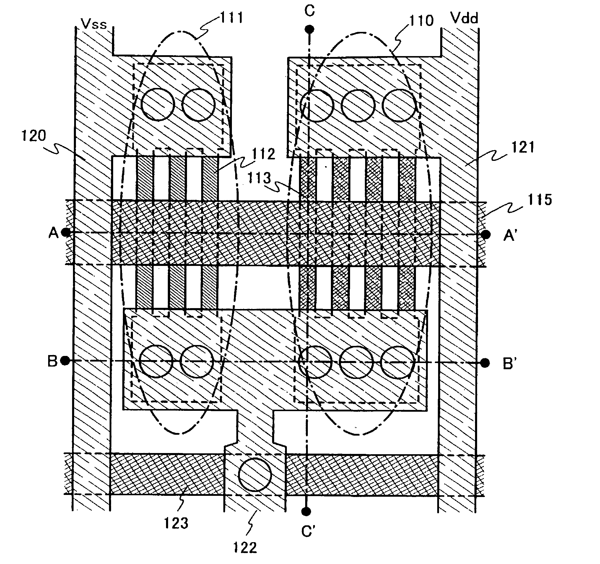
The TFT formed by using the present manufacturing method can be implemented to a driver circuit of a semiconductor display device and the other circuit included in the semiconductor display device. In this embodiment, a description will be made of a structure of a controller of a semiconductor display device formed according to the manufacturing method of the present invention. Note that in this embodiment, a structure of the controller of a light emitting device using an OLED (organic light emitting device) will be described. However, the present invention is not limited to this but may adopt a controller of the liquid crystal display device and those of other semiconductor display devices. Also, it may be a drive circuit other than the controller and a semiconductor device other than the display device is also possible.
FIG. 14 shows the structure of the controller of this embodiment. The controller includes an interface (I / F) 650, a panel link receiver 651, a phase locked loop (PL...
PUM
 Abstract
Description
Claims
Application Information