Hetero-bipolar transistor

a transistor and bipolar technology, applied in the field of heteropolar transistors, can solve the problems of reducing the current gain of the transistor and increasing the base curren

Inactive Publication Date: 2005-04-05
SUMITOMO ELECTRIC IND LTD
View PDF12 Cites 1 Cited by
  • Summary
  • Abstract
  • Description
  • Claims
  • Application Information

AI Technical Summary

Problems solved by technology

This causes an increase of the base current, and acco

Method used


Image

  • Hetero-bipolar transistor
  • Hetero-bipolar transistor
  • Hetero-bipolar transistor

Examples


first embodiment

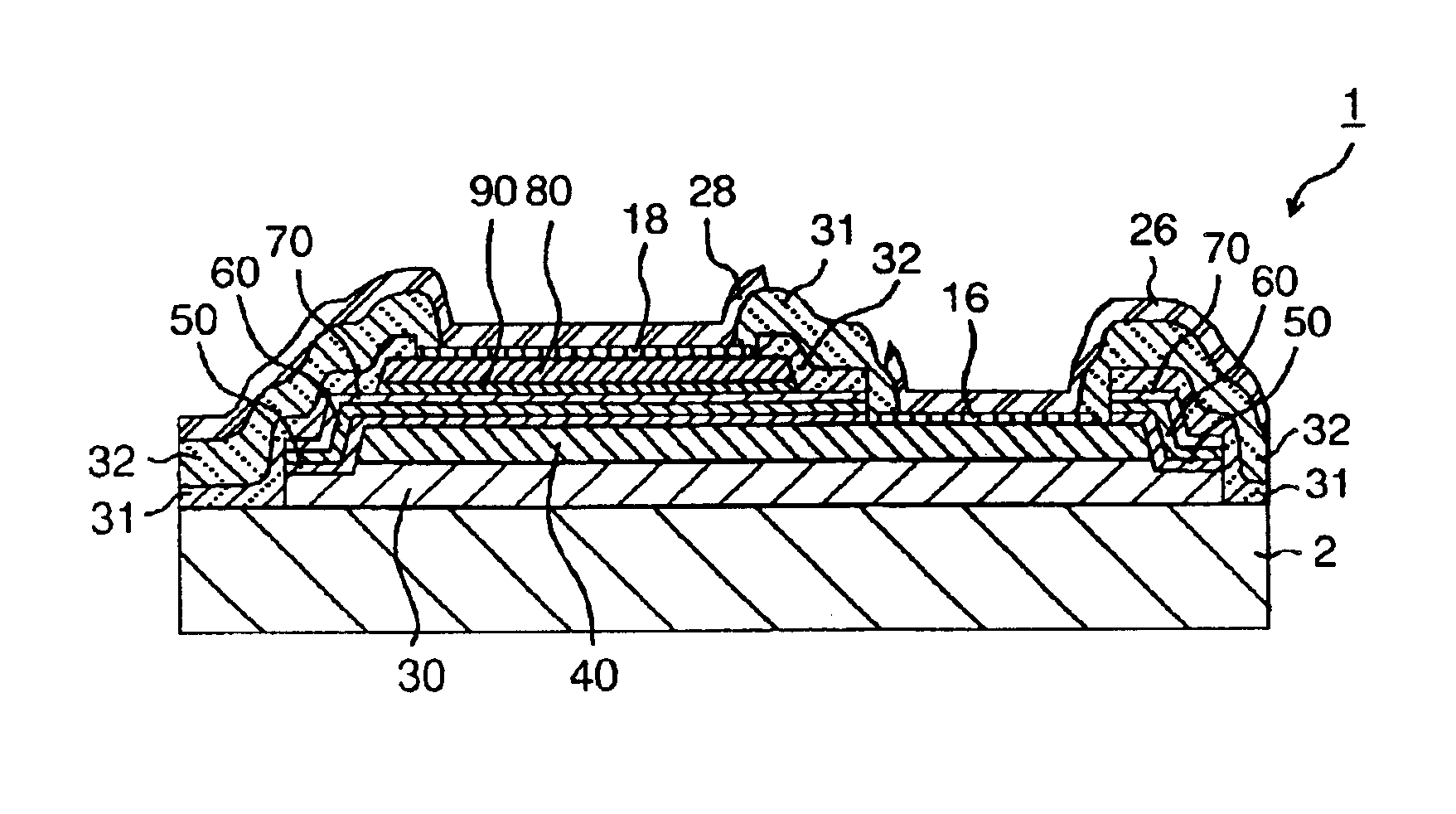
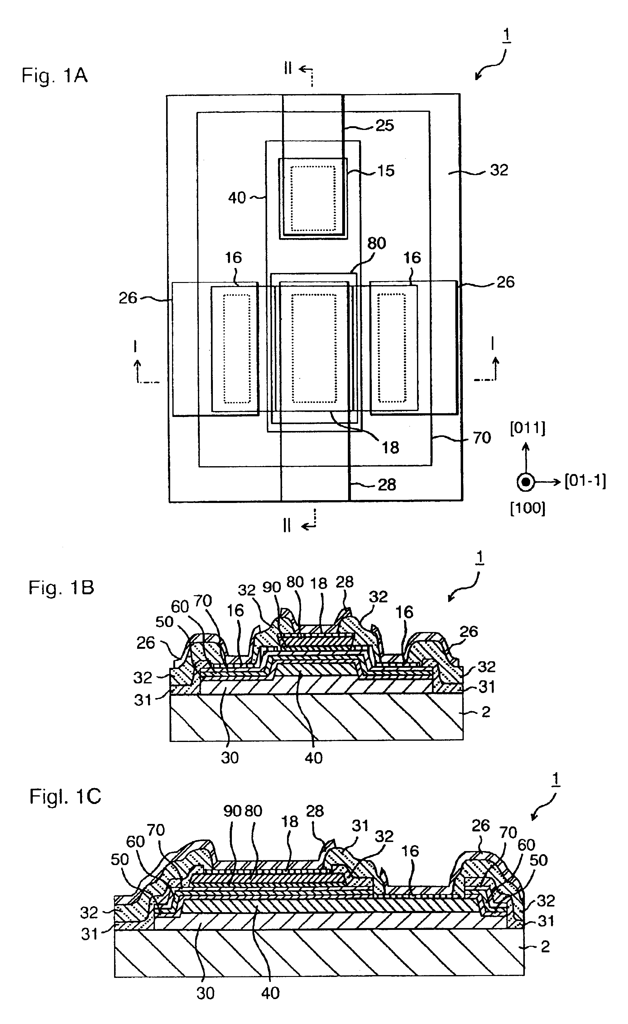
FIG. 1A shows a plan view of an HBT according to a first embodiment of the present invention. FIG. 1B and FIG. 1C are cross-sectional views taken along line I—I and line II—II in FIG. 1A, respectively. In FIG. 1A, line I—I is along [01-1] and line II—II is along [011] in crystal direction.

The HBT 1 comprises a series of layers: A buffer layer 30 on the (100) surface of a semi-insulating InP substrate, a sub-collector layer 40 on the buffer layer, a collector layer 50 on the buffer layer and the sub-collector layer, a base layer 60 on the collector layer, an emitter layer 70 on the base layer, and an emitter contact layer 80 on the emitter layer. The emitter layer 70 and the emitter contact layer sandwich an intermediate layer 90 therebetween.

The buffer layer 30 is an undoped InxGa1−xAs (hereinafter InGaAs) with a thickness from 300 nm to 500 nm. The sub-collector layer 40 is an n-type InGaAs with a thickness from 300 nm to 500 nm doped with Si by the range of 0.5×1019 cm−3 to 2.0×10...

second embodiment

The second embodiment of the HBT according to the present invention is the same as the first embodiment except for the electron distribution in the emitter contact layer and the intermediate layer.

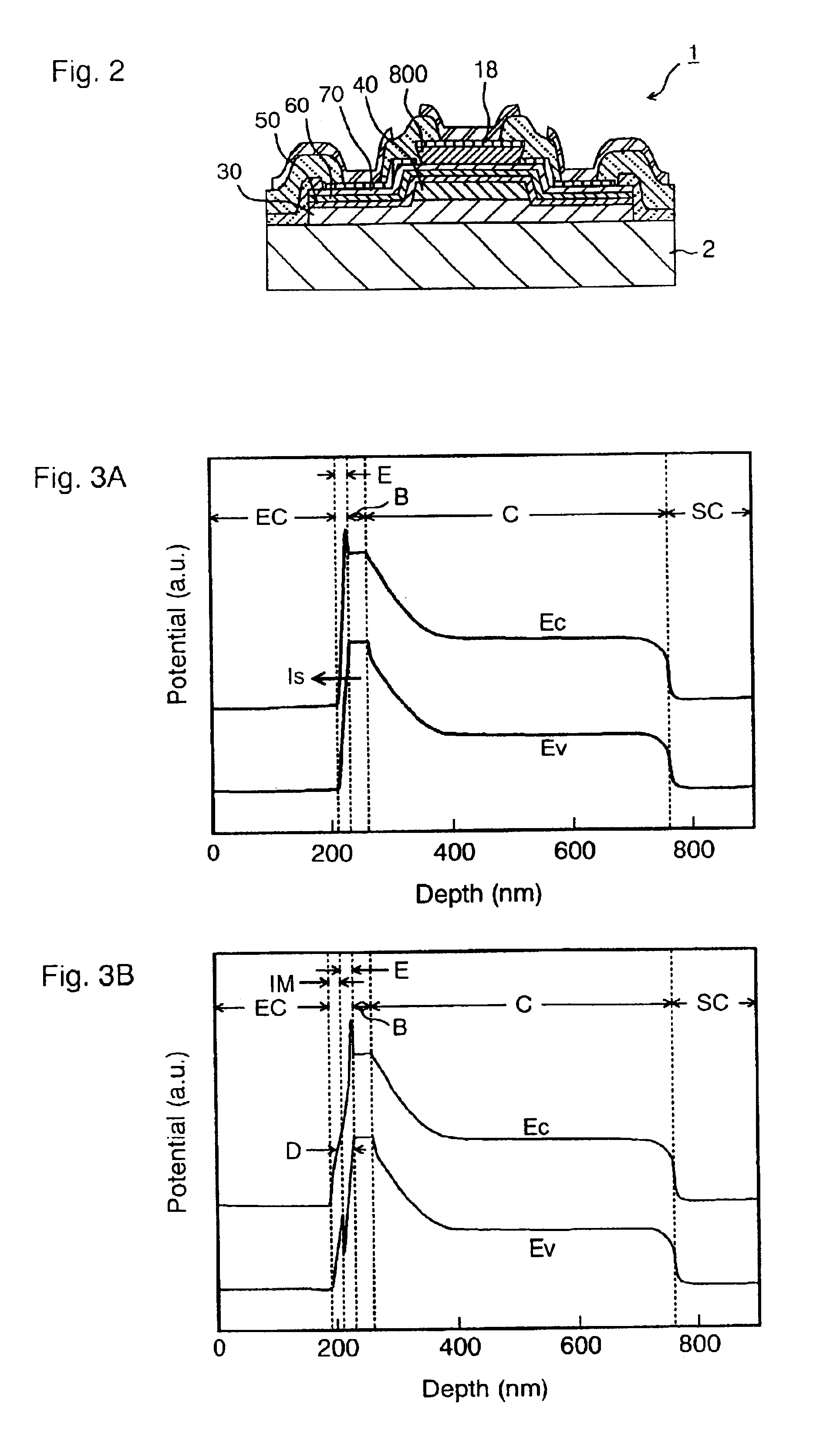
FIG. 7A shows a typical electron distribution in the emitter contact layer 81 and the intermediate layer 91 in the second HBT 100. As shown in FIG. 7A, the electron concentration in the intermediate layer 91 is smaller than that in the emitter contact layer 81. The amount of electron concentration is 1×1018 cm−3 or smaller, and monotonically increases from the interface of the emitter layer 80 to the emitter contact layer 81. The minimum concentration is about 4×1017 cm−3 at the interface of the emitter layer 70. The distribution in the emitter contact layer 81 also monotonically increases from the interface of the intermediate layer 91 to the emitter electrode 18. The maximum concentration at the emitter electrode reaches 2×1019 cm−3.

Under the distribution thus described, the depletion re...


PUM


Abstract

The present invention provides a Hetero-Bipolar Transistor that suppresses a recombination current between electrons in the conduction band of an emitter and holes in the valence band of a base, which results on an enhancement of the current gain of the transistor. The HBT according to the present invention comprises a semi-insulating semiconductor substrate and a series of semiconductor layers on the substrate. The semiconductor layers are a buffer layer, a sub-collector layer a collector layer, a base layer, an emitter layer, an emitter contact layer, and an intermediate layer between the emitter layer and the emitter contact layer. The emitter layer has a carrier concentation of 1.0×1019 cm−3.

Description

BACKGROUND OF THE INVENTION1. Field of the InventionThis invention relates to a hetero-bipolar transistor (HBT), particularly to an HBT made of group III-V compound semiconductor materials.2. Related Prior ArtA tunneling emitter bipolar transistor (TEBT) is a device that achieves a superior high frequency performance and a current gain. Such characteristics of the TEBT are reported in the IEEE Electron Device Letters, vol. EDL-7 pp. 416, (1986) and Applied Physics Letters, vol. 50(26) pp. 1915 (1987). The former document discloses the structure of the TEBT in which a base and an emitter are made of GaAs and a tunnel emitter of AlGaAs is inserted therebetween with a thickness of 3 nm to 20 nm. In this configuration, electrons can tunnel through the AlGaAs emitter layer, while the hole injection from the base layer to the emitter layer is suppressed because the tunnel probability for the hole is smaller as compared with electrons therethrough. Moreover, even in increasing the hole con...

Claims


Application Information

Patent Timeline
IPC IPC(8): H01L21/331H01L21/02H01L29/737
CPCH01L29/66318
Inventor YANAGISAWA, MASAKI
Owner SUMITOMO ELECTRIC IND LTD
Why Eureka
Try Eureka