

Flash with finger-like floating gate
a floating gate and finger-like technology, applied in the field of memory cells, can solve the problems of high voltage and excessive circuitry, affecting affecting the accuracy of control gates, etc., to achieve the effect of increasing reliability, and increasing the coupling ratio of control gates and floating gates
- Summary
- Abstract
- Description
- Claims
- Application Information
AI Technical Summary
Benefits of technology
Problems solved by technology
Method used
Image

Examples
Embodiment Construction
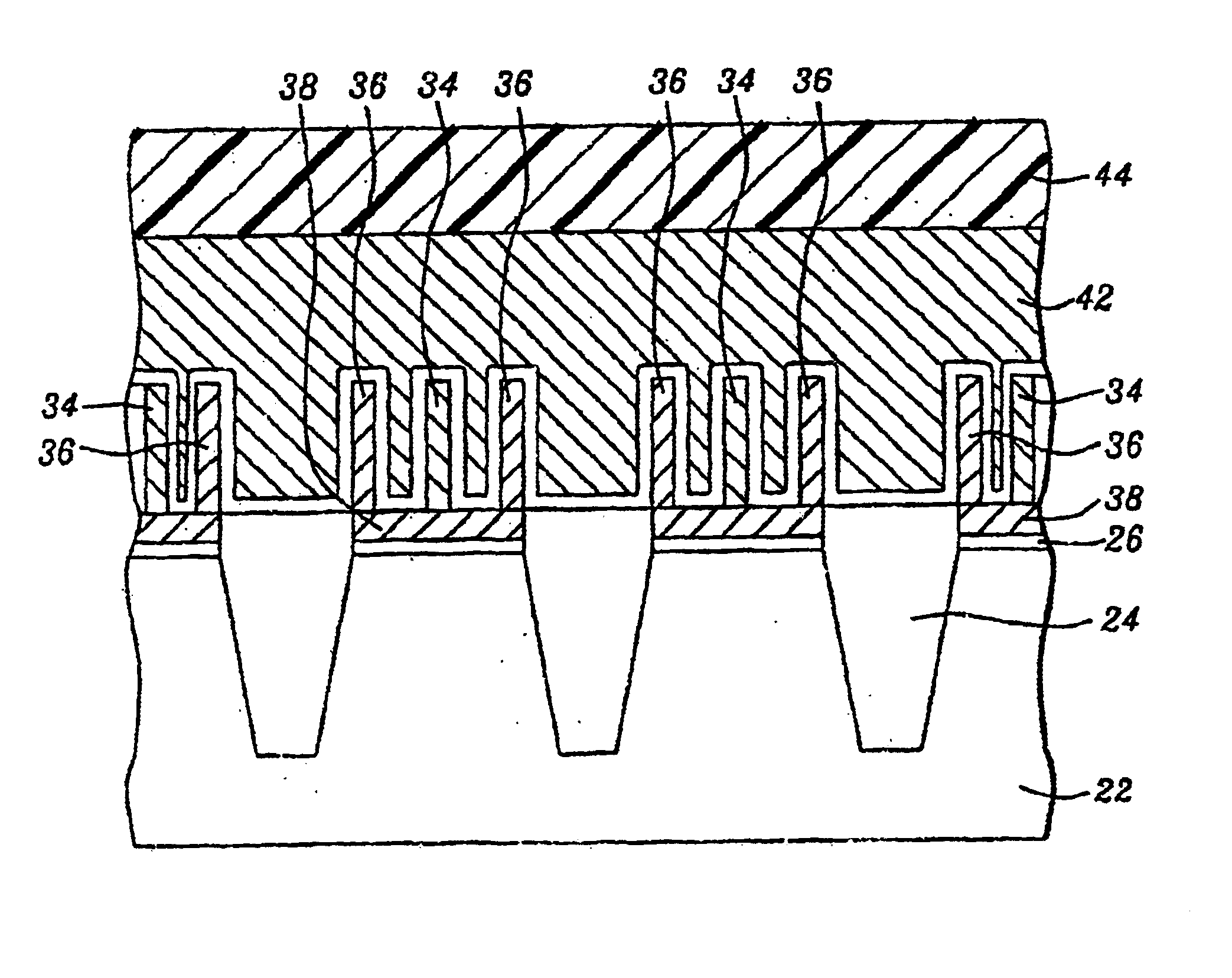
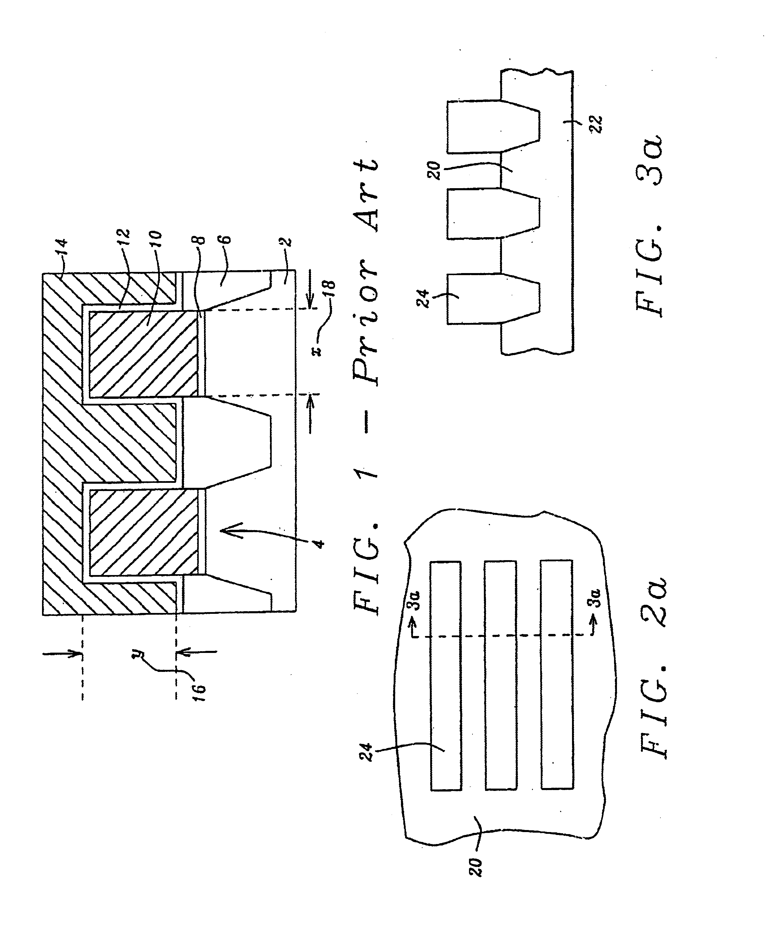
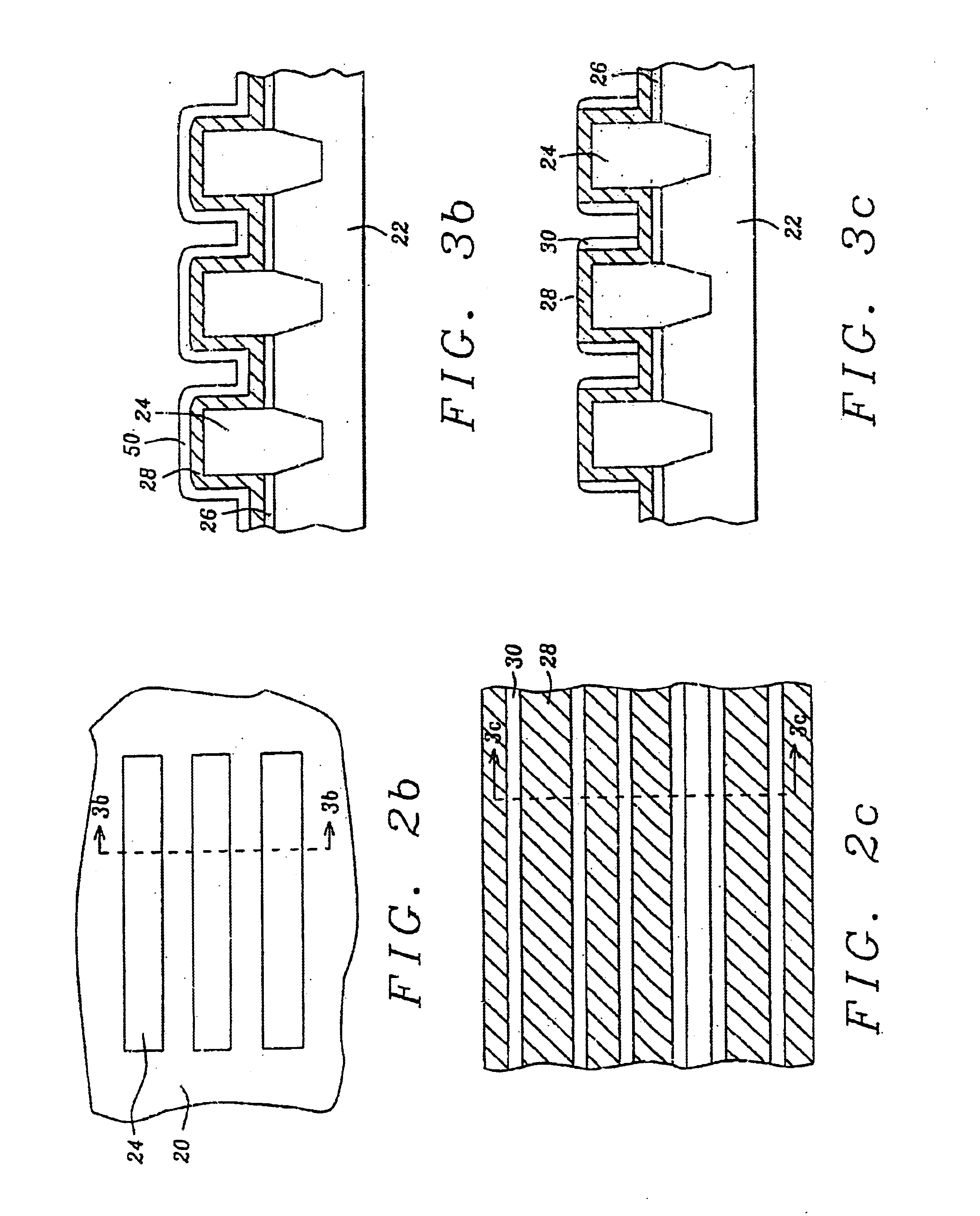
Preferred embodiments of the invention are well described with the aid of FIGS. 2a-2i and 3a-3i. A method of fabricating a finger-like floating gate is presented in FIGS. 2a-2i, where top views are presented at successive stages of the process and in FIGS. 3a-3i, which show the corresponding cross-sectional views. As shown in FIGS. 2a and 3a, active regions, 20, are defined on a semiconductor region, 22, which preferably is a p-type silicon region, using raised isolation regions, 24, such as shallow trench isolation, STI, regions. A floating gate dielectric layer, 26, is then formed over the active regions to a thickness of about 100 Angstroms. Preferably the floating gate dielectric layer is a thermally grown oxide. The gate dielectric layer serves as the dielectric layer between the semiconductor region and the floating gate. Deposition of a blanket first conductive layer, 28, follows, over the gate dielectric layer, 26, that covers the active regions and over the top and exposed ...
PUM
 Abstract
Description
Claims
Application Information