Unified SRAM cache system for an embedded DRAM system having a micro-cell architecture

a microcell architecture and cache system technology, applied in the field of integrated circuit (ic) design, can solve the problems of not being area efficient in srom and the edram system having several small sram macros, and achieve the effect of wide internal bus width and wide data bandwidth

Inactive Publication Date: 2005-04-05
GLOBALFOUNDRIES U S INC
View PDF3 Cites 14 Cited by
  • Summary
  • Abstract
  • Description
  • Claims
  • Application Information

AI Technical Summary

Benefits of technology

An aspect of the present invention is to provide a unified SRAM cache system incorporating several SRAM macros of an embedded DRAM (eDRAM) system and their functions, so that each incorporated SRAM macro can be independently accessed without interfering with the other incorporated SRAM macros within the unified SRAM cache system. The eDRAM system includes a micro-cell architecture, a wide data bandwidth and a wide internal bus width.
Another aspect of the present invention is to provide a unified SRAM cache system incorporating several SRAM macros of an eDRAM system, where the incorporated SRAM macros share a single set of support circuits without compromising the performance of the eDRAM system.

Problems solved by technology

Similar to a fuse register array, the SROM is not an area efficiency design.
An eDRAM system having several small SRAM macros is not area efficient.

Method used


Image

  • Unified SRAM cache system for an embedded DRAM system having a micro-cell architecture
  • Unified SRAM cache system for an embedded DRAM system having a micro-cell architecture
  • Unified SRAM cache system for an embedded DRAM system having a micro-cell architecture

Examples


Embodiment Construction

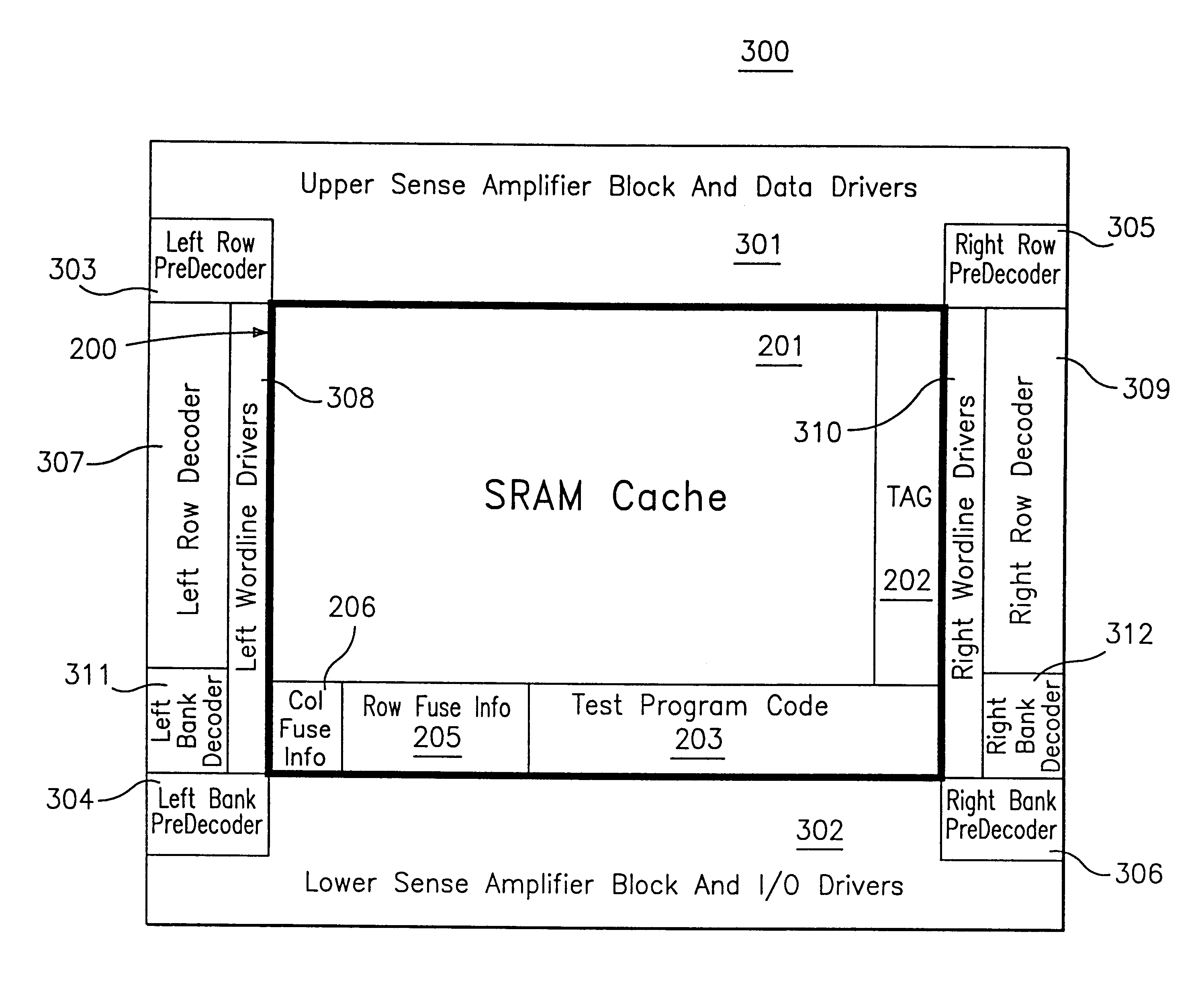
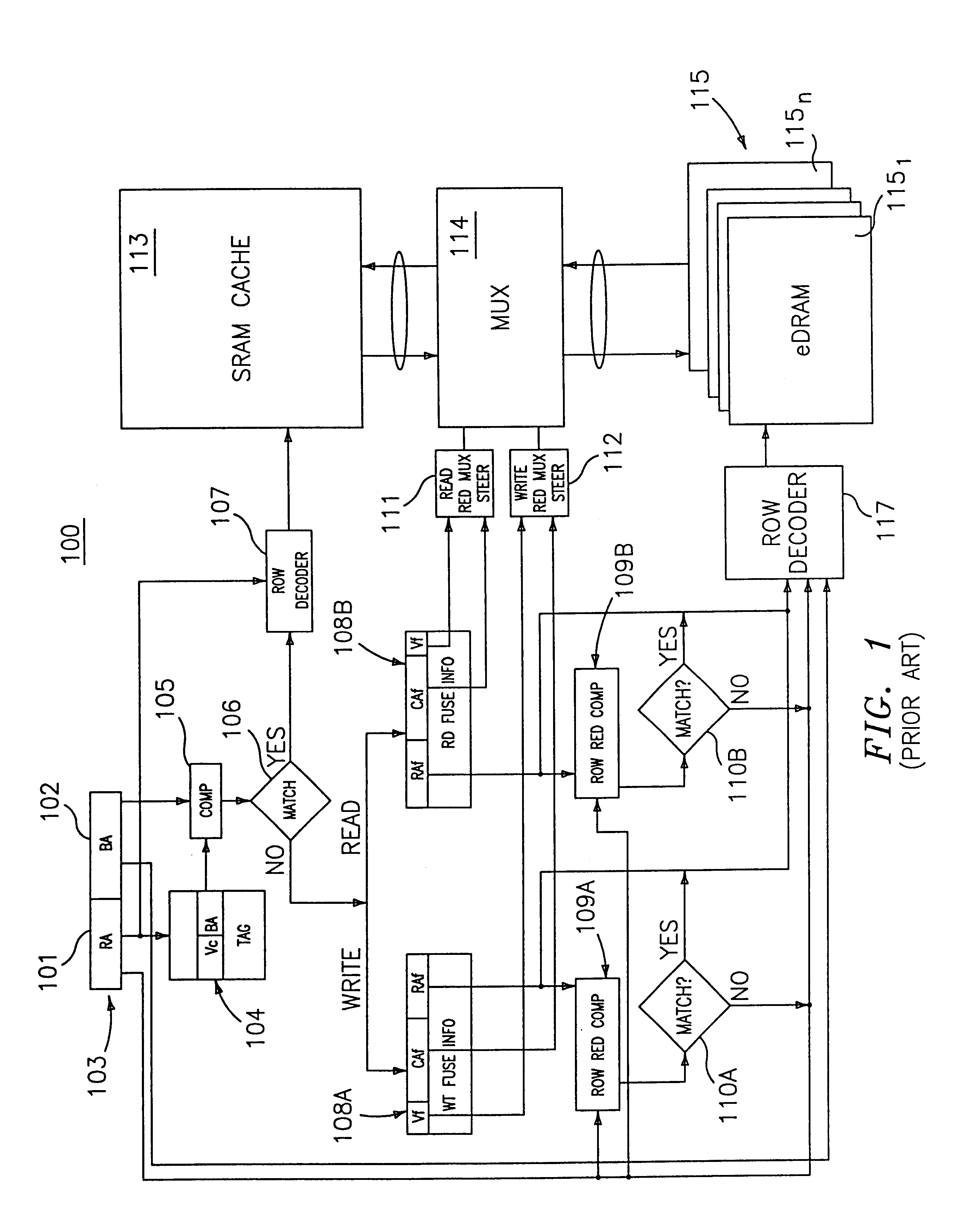
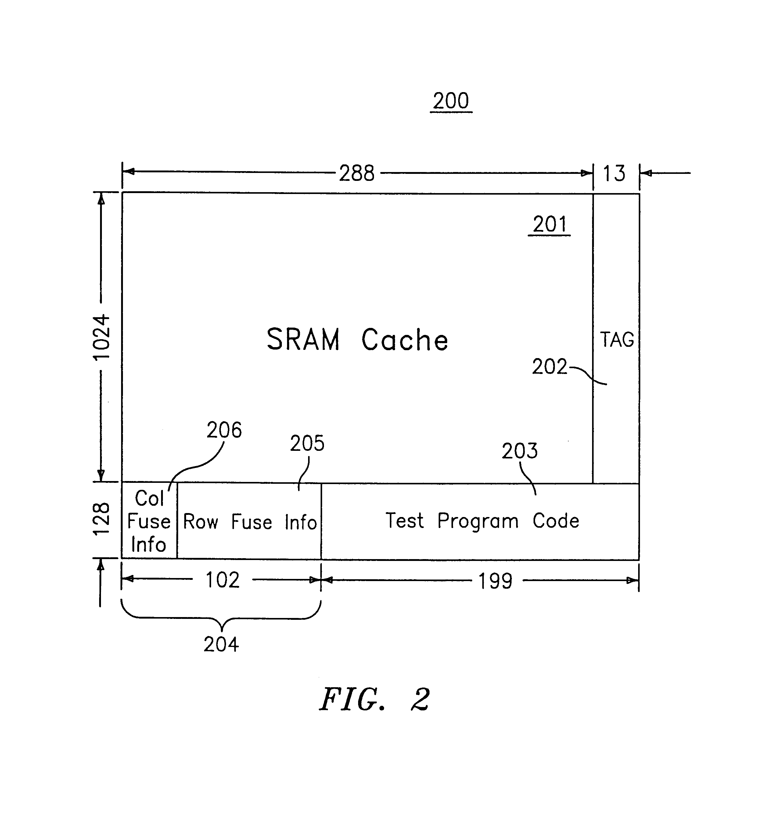
The present invention provides a unified SRAM cache system for an embedded DRAM (eDRAM) having a micro-cell architecture, a wide data bandwidth and wide internal bus width. A description will now be given as to the operation of an embedded DRAM macro. In order to save chip area, the purpose of this description is to illustrate that the unified SRAM cache system of the present invention can be used to replace several SRAM macros without jeopardizing the eDRAM operation.

With reference to FIG. 1, there is shown a block diagram of a prior art high-speed eDRAM macro system having a micro-cell architecture designated generally by reference numeral 100. When an incoming address 103 is received from a CPU or memory controller, it contains a row address field (RA) 101 and a bank address field (BA) 102. The row address field 101 is used to decode a TAG block cache 104 to find out whether the data is currently stored in an SRAM cache 113. If the valid bit Vc of the decoded row of the TAG block...


PUM


Abstract

A unified SRAM cache system is provided incorporated several SRAM macros of an embedded DRAM (eDRAM) system and their functions. Each incorporated SRAM macro can be independently accessed without interfering with the other incorporated SRAM macros within the unified SRAM cache system. The incorporated SRAM macros share a single set of support circuits, such as row decoders, bank decoders, sense amplifiers, wordline drivers, bank pre-decoders, row pre-decoders, I / O drivers, multiplexer switch circuits, and data buses, without compromising the performance of the eDRAM system.

Description

FIELD OF THE INVENTIONThis invention relates to the field of integrated circuit (IC) design. Specifically, it relates to a unified SRAM cache system for an embedded DRAM (eDRAM) system having a micro-cell architecture, a wide data bandwidth and a wide internal bus width.BACKGROUND OF THE INVENTIONEmbedded DRAMs (eDRAMs) with wide data bandwidth and wide internal bus width have been proposed to be used as L2 (level-2) cache to replace pure SRAM cache. Since each DRAM memory cell is formed by a transistor and a capacitor, the size of DRAM cache is significantly smaller than that of SRAM cache. In order to meet performance requirements, DRAMs are made of a plurality of blocks or micro-cells. A block is a small DRAM array unit formed by a plurality of wordlines (e.g., from 64 to 256) and a plurality of bitline pairs (e.g., from 64 to 256). The size of a block is much smaller (e.g., 16× to 256×) than that of a bank of a conventional stand-alone DRAM. Only one block of the eDRAMs is activ...

Claims


Application Information

Patent Timeline
Patent Type & Authority Patents(United States)
IPC IPC(8): G06F12/08
CPCG06F12/0893
Inventor HSU, LOUIS L.JOSHI, RAJIV V.
Owner GLOBALFOUNDRIES U S INC
Why Eureka
Try Eureka