Semiconductor memory device

a memory device and semiconductor technology, applied in the direction of information storage, static storage, digital storage, etc., can solve the problems of slowness, prolonged refresh operation and subsequent read/write operation, and difficulty in completing refresh operation, so as to increase the speed of the semiconductor memory device and speed up the internal operation

a memory device and semiconductor technology, applied in the direction of information storage, static storage, digital storage, etc., can solve the problems of slowness, prolonged refresh operation and subsequent read/write operation, and difficulty in completing refresh operation, so as to increase the speed of the semiconductor memory device and speed up the internal operation

US6876592B2Inactive Publication Date: 2005-04-05RENESAS ELECTRONICS CORP

Image

  • Semiconductor memory device
  • Semiconductor memory device
  • Semiconductor memory device

Examples


fourth embodiment

le of the structure of a semiconductor memory device according to the present invention with respect to the hierarchical word line structure.

[0050]FIG. 11 is a block diagram showing the structure of a semiconductor memory device according to a fifth embodiment of the present invention.

[0051]FIG. 12 is a timing chart showing the operation of a semiconductor memory device according to a fifth embodiment of the present invention.

[0052]FIG. 13 is a block diagram showing the structure of a semiconductor memory device according to a sixth embodiment of the present invention.

[0053]FIG. 14 is a timing chart showing the operation of a semiconductor memory device according to a sixth embodiment of the present invention.

[0054]FIG. 15 is a block diagram showing the structure of a semiconductor memory device for realizing the address access method according to the background art.

[0055]FIG. 16 is a timing chart showing the operation of the semiconductor memory device shown in FIG. 15.
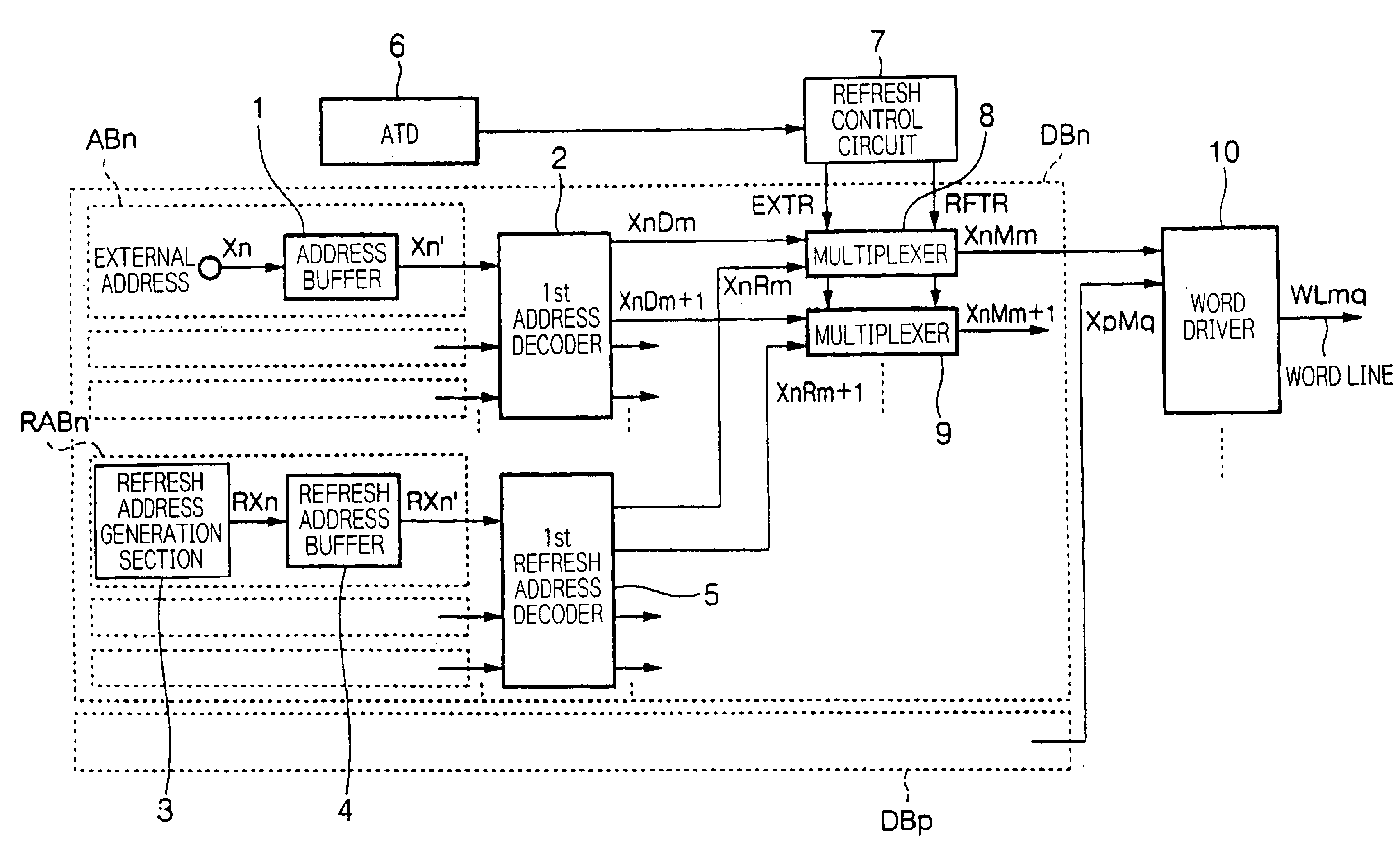
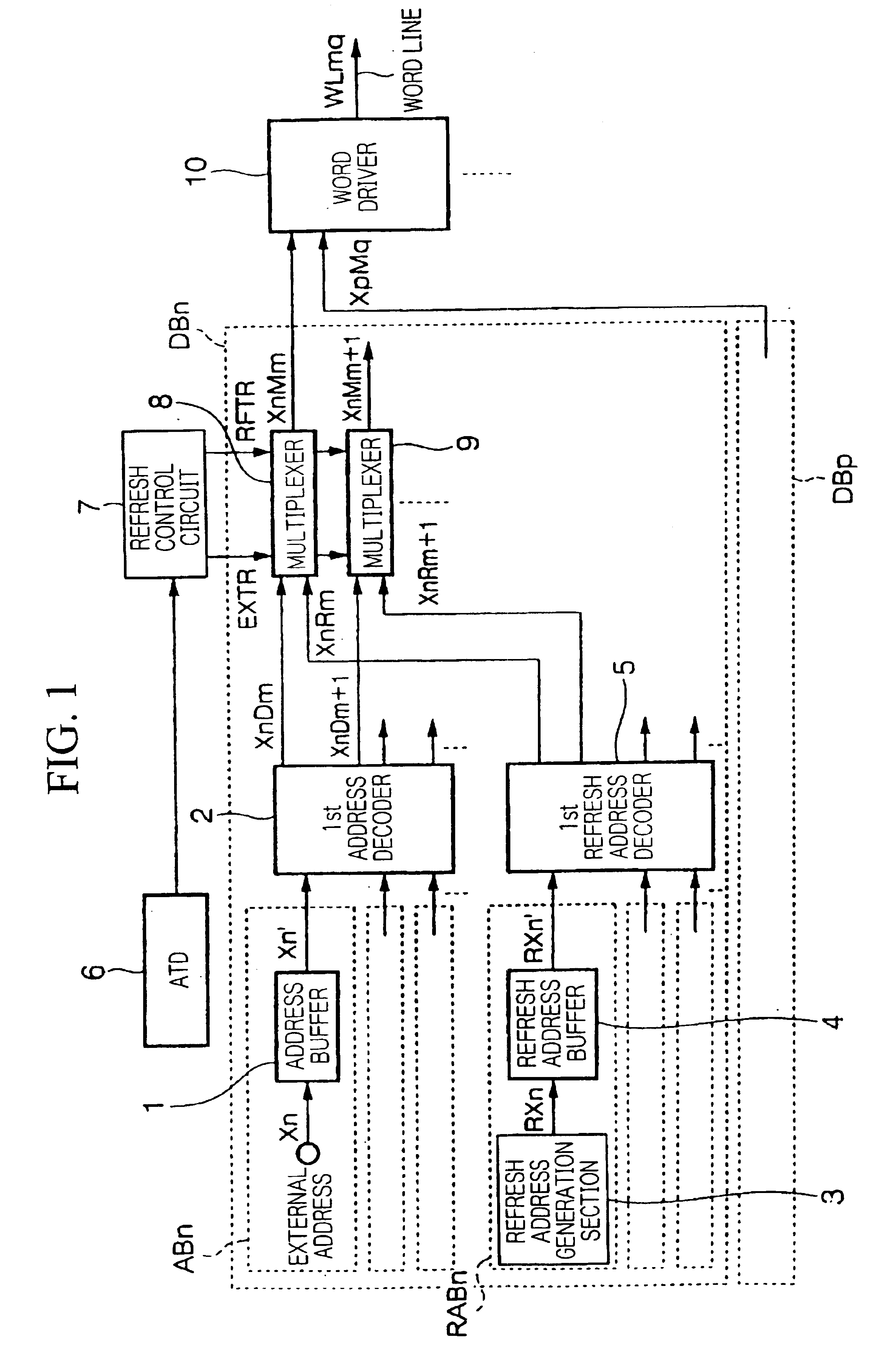
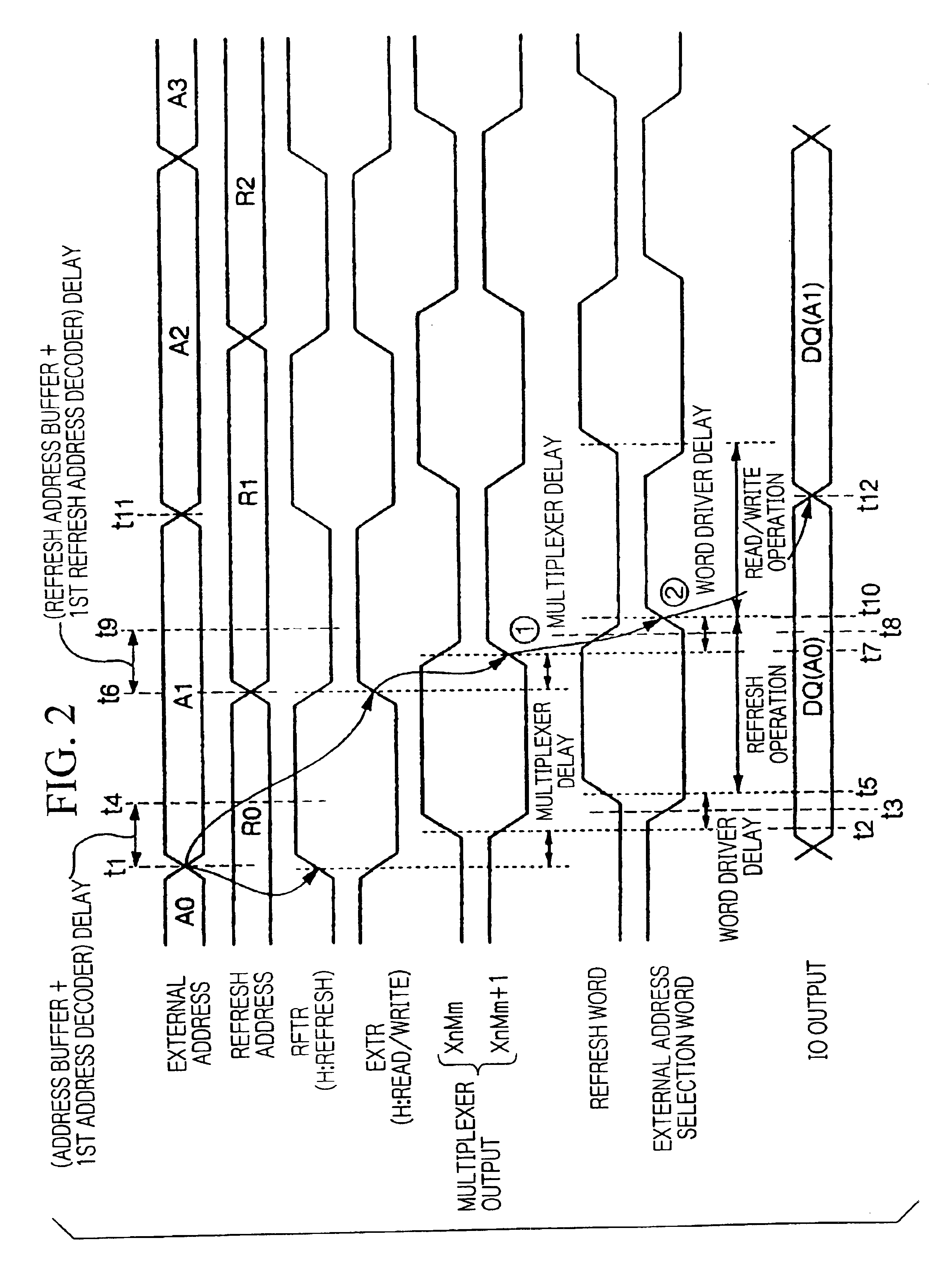
[0056]FIG. 1...


PUM


Abstract

A semiconductor memory device capable of accelerating address access and shortening cycle time is provided. A first address decoder (2) and first refresh address decoder (5) respectively decode an external address (Xn) supplied from outside the semiconductor memory device and a refresh address (RXn) used for refreshing within the semiconductor memory device. A multiplexer (8) selects the external address side decode signal (XnDm) or the refresh address side decode signal (XnRm) and outputs the signal as a decode signal (XnMm) based on an external address transmission signal (EXTR) and refresh address transmission signal (RFTR) so that a refresh operation and a read / write operation is performed continuously within one memory cycle. A word driver (10) then decodes decode signals (XnMm, XpMq) selected with multiplexer (8) and so forth, and activates a word line (WLmq).

Description

TECHNICAL FIELD[0002]The present invention relates to a semiconductor memory device that uses DRAM (Dynamic Random Access Memory) cells that must be refreshed to retain data as memory cells, and more particularly, to an address access method that is suitable when operating a semiconductor memory device that uses DRAM cells in the form of general-purpose SRAM (static RAM) specifications (asynchronous specifications). In addition, the present invention relates to an address access method that is also applicable to a semiconductor memory device equipped with memory cells array that are accessed in the absence of a failure, and a spare memory cell array for remedying a failure by replacing a failed memory cell and so forth on that memory cell array.BACKGROUND ART[0003]Semiconductor memory devices have been proposed that detect the transition of an external address supplied from outside a semiconductor memory device, refresh the memory cells indicated by a refresh address generated withi...

Claims


Application Information

Patent Timeline
05 Apr 2005
Publication
US6876592B2
IPC
G11C11/408; G11C11/406; G11C11/401; G11C11/403; G11C11/407; G11C29/04
CPC
G11C11/4087; G11C11/406; G11C11/401
Inventors
TAKAHASHI, HIROYUKI; INABA, HIDEO