Method of forming high voltage junction in semiconductor device

Inactive Publication Date: 2005-04-12
SK HYNIX INC
View PDF11 Cites 9 Cited by
  • Summary
  • Abstract
  • Description
  • Claims
  • Application Information

AI Technical Summary

Benefits of technology

The present invention is contrived to solve the above problems and an object of the present invention is to provide a method of forming a high voltage junction in a semiconductor device that can reduce the sheet resistance by prohibiting diffusion of an impurity, prohibit a channeling phenomenon by lowering the depth of the junction, and remove crystal defects by sufficiently activating an impurity since a subsequent annealing process for activation can be performed at a high temperature, and t

Problems solved by technology

Therefore, from a viewpoint that the effective length (Leff) is not reduced even though a high voltage junction breakdown of over 20V is usually required in the NAND device, it is impossible to unlimitedly increase the DDD junction.
Thus, the leakage current of the junction structure is increased.
However, if the high-temperature annealing process is performed, the high voltage junction structure having a shallow depth could not be formed due to diffusion of the impurity.
Further, as the acti

Method used


Image

  • Method of forming high voltage junction in semiconductor device
  • Method of forming high voltage junction in semiconductor device
  • Method of forming high voltage junction in semiconductor device

Examples


Embodiment Construction

The present invention will be described in detail by way of a preferred embodiment with reference to accompanying drawings, in which like reference numerals are used to identify the same or similar parts.

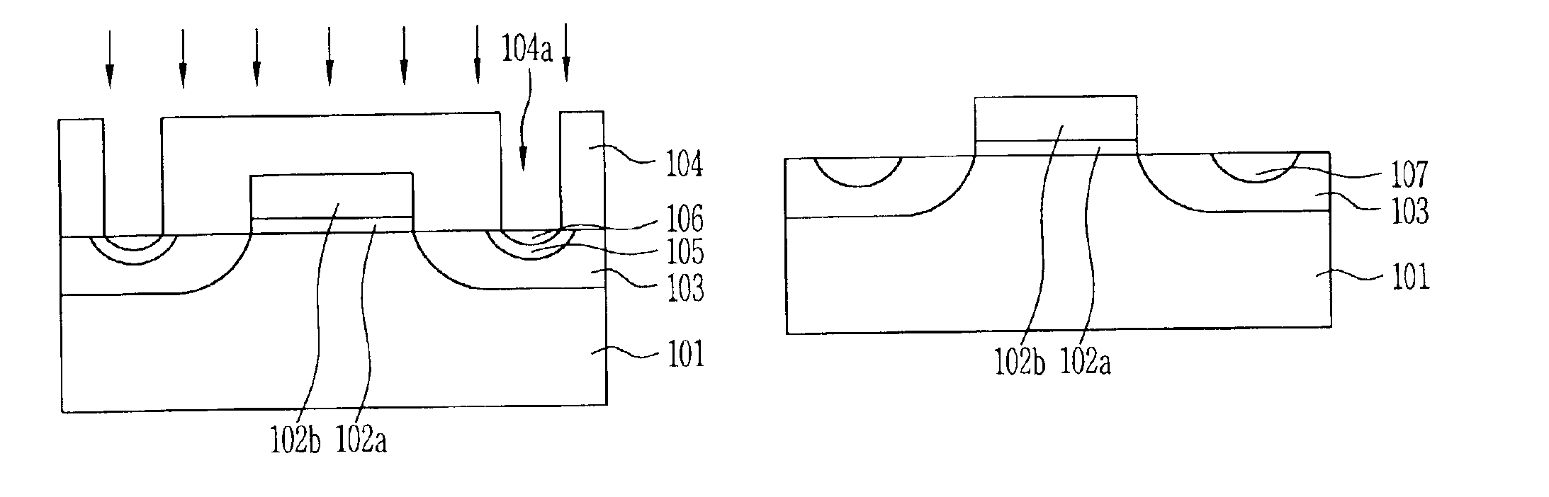
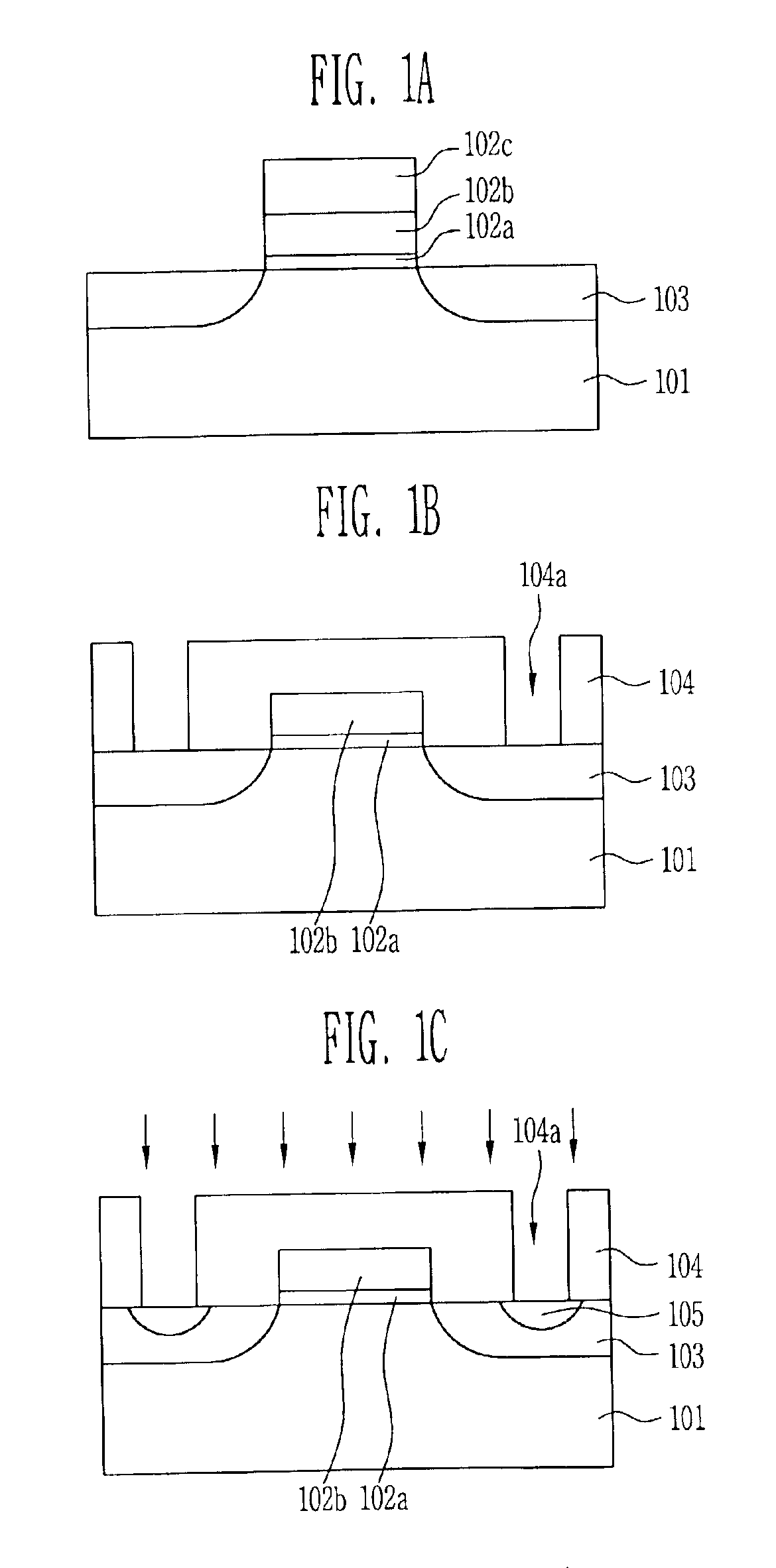
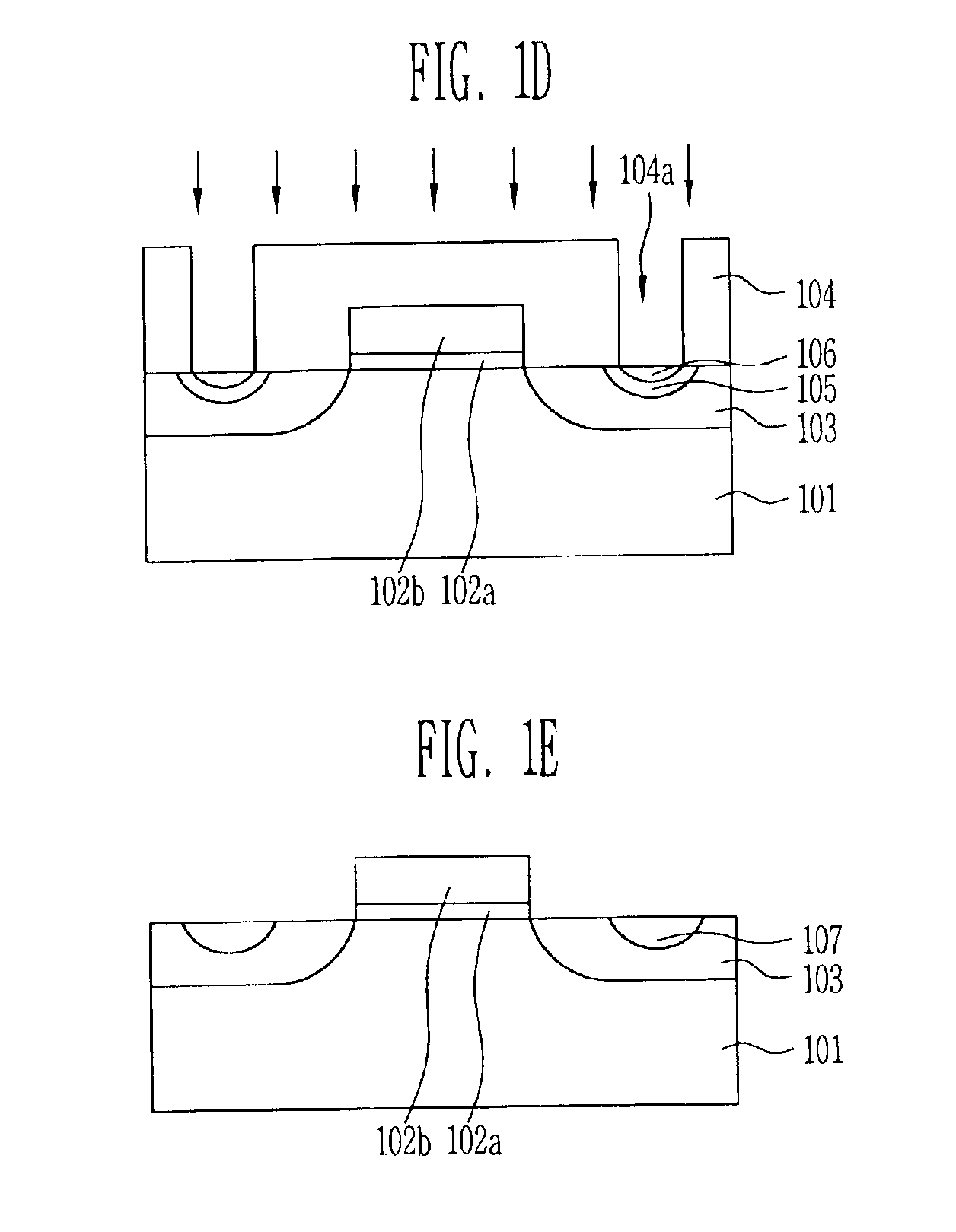
FIG. 1A through FIG. 1E are cross-sectional views of semiconductor devices for explaining a method of forming a high voltage junction in the semiconductor device according to a preferred embodiment of the present invention.

Referring now to FIG. 1A, a stack structure of a gate oxide film 102a, a gate 102b and a hard mask 102c is formed on a semiconductor substrate 101. After the stack structure is then patterned, double diffused drain (DDD) junctions 103 are formed in the semiconductor substrate 101 at both sides of the gate 102b by means of an ion implantation process.

In the above, the gate oxide film 102a is formed by a wet oxidization method. In order to increase the breakdown voltage of the junction to a high voltage (for example, 40V), the junction is formed in thickness of 200 ...


PUM


Abstract

The present invention relates to a method of forming a high voltage junction in a semiconductor device. The method includes forming a double diffused drain junction, and making amorphous the double diffused drain junction to a first depth by implanting an impurity having a high atomic weight than an impurity injected into the double diffused drain junction, implanting an impurity so that the concentration of the concentration of an impurity to a second depth lower than the first depth and then activating the impurities. Thus, the present invention can reduce the sheet resistance by prohibiting diffusion of an impurity, prohibit a channeling phenomenon by lowering the depth of the junction, and remove crystal defects by sufficiently activating an impurity and since a subsequent annealing process for activation can be performed at a high temperature, and thus improve reliability of a process and an electrical characteristic of the device.

Description

BACKGROUND OF THE INVENTION1. Field of the InventionThe invention relates generally to a method of forming a high voltage junction in a semiconductor device. More particularly, the invention relates to a method of forming a high voltage junction in a semiconductor device capable of minimizing crystal defects in a process of forming a junction structure to which a high voltage is applied and forming a junction structure of a shallow depth having a low breakdown voltage and a low sheet resistance.2. Description of the Prior ArtA semiconductor device may be classified into a high voltage device and a low voltage device depending on its driving voltages. Of them, the high voltage device includes a high voltage transistor used in a charge pump circuit for generating a program voltage or an erase voltage of a high voltage in the flash memory device. A junction structure of the high voltage device such as the high voltage transistor (for example, source and drain of the high voltage transi...

Claims


Application Information

Patent Timeline
IPC IPC(8): H01L21/265H01L21/02H01L29/66H01L29/78H01L21/336H01L29/76
CPCH01L21/26513H01L29/7833H01L29/66575H01L29/76
Inventor PARK, JEONG HWANKWAK, NOH YEAL
Owner SK HYNIX INC
Why Eureka
Try Eureka