Multi-level integrated circuit for wide-gap substrate bonding

a technology of integrated circuits and substrates, applied in the direction of fluid speed measurement, instruments, coatings, etc., can solve the problems of large gaps between substrates, limited gap spacing using conventional processes, and inability to deposit the large thickness required for some applications,

Inactive Publication Date: 2005-04-12
TAIWAN SEMICON MFG CO LTD
View PDF19 Cites 52 Cited by
  • Summary
  • Abstract
  • Description
  • Claims
  • Application Information

AI Technical Summary

Benefits of technology

[0010]An integrated circuit includes a substrate having an etched surface and a non-etched surface. The etched surface contains circuit elements and the non-etched surface contains a bonding surface. The non-etched surface is located at a predetermined height from the etched surface. Bonding this integrated circuit with another substrate creates a wide-gap between the substrates that is preferably evacuated and hermetically sealed.

Problems solved by technology

Conventional integrated circuit (IC) fabrication techniques to apply the spacer material, such as sputtering of metal films, cannot deposit large thickness required for some applications.
Because thicker sputtered metal films suffer from stress and flaking, the amount of the gap spacing using conventional processes is limited to thicknesses less than a few microns.
However, some applications require large gaps between the substrates, for example, such as to provide for high voltage separation or isolation.
Any defect caused by the stress or flaking of sputtered metal films can result in a leak, thus compromising the vacuum and thereby ultimately causing the product to likely fail.
However, this etching of the electro-plated layer can damage other materials such as thin-film layers that have been previously applied to the substrate.
Therefore, electroplating has not been an effective option.
By adding spacer material, such as sputtered metal films or electro-plated metals, the interconnections are difficult to make as the additional thickness of the spacer material must be compensated for when making the interconnections.

Method used


Image

  • Multi-level integrated circuit for wide-gap substrate bonding
  • Multi-level integrated circuit for wide-gap substrate bonding
  • Multi-level integrated circuit for wide-gap substrate bonding

Examples


exemplary embodiment 42

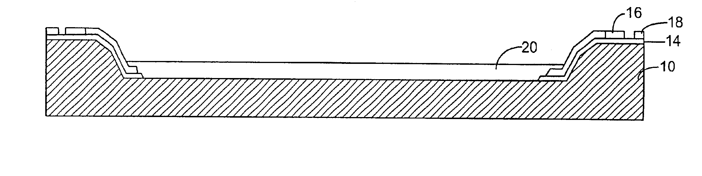
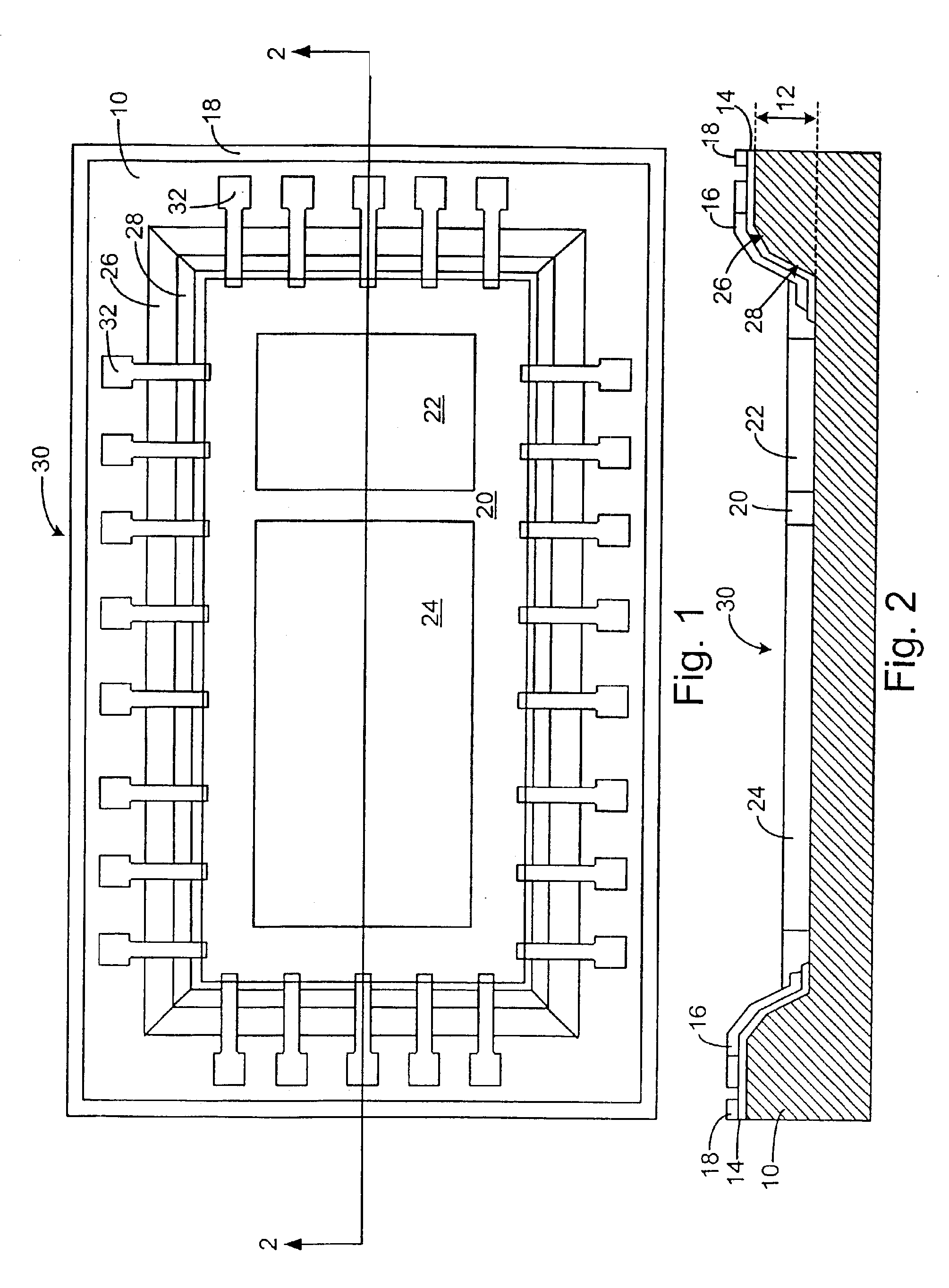
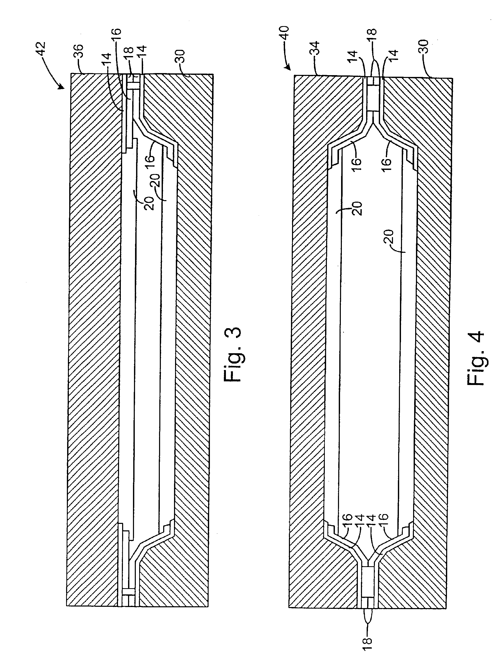
[0032]FIG. 3 is a first exemplary embodiment 42 of a micro-machined system using a multi-level integrated circuit embodied using the invention. In this embodiment, a first IC 30 has been etched to remove a portion of the substrate material and then processed with semiconductor thin-film layers 20 to create circuit elements. The circuit elements on the etched surface of IC 30 are coupled to the non-etched surface using conductive layer 16 as an interlevel conductor 32 (see FIG. 1). The conductive layer 16 is isolated from the substrate using a dielectric layer 14. The first IC 30 is shown bonded to a conventional substrate, second IC 36. The second IC 36 preferably also has been processed with semiconductor thin-film layers 20 to create circuit elements. These circuit elements are also connected with a conductive layer 16 to align with the conductive layer 16 of first IC 30. A seal 18 is shown here to provide preferably, but optionally, a hermetic seal around the peripheral edge of t...

exemplary embodiment 44

[0035]FIG. 5 is a third exemplary embodiment 44 of a micro-machined system with two multi-level integrated circuits embodied using the invention. In this embodiment, a fourth IC 38, having a surface area smaller than the surface area of first IC 30, is bonded to first IC 30 using an alternative seal 52 that is also preferably an adhesive. Optionally, the seal 18 of the earlier embodiments could be used in place of or in conjunction with alternative seal 52. The alternative seal 52 preferably provides a hermetic seal and is preferably applied after the first IC 30 and the fourth IC 38 are bonded together or optionally applied during the bonding process. In this embodiment, another feature is that conductive layer 16 on first IC 30 can extend to beyond the peripheral edge of fourth IC 38 to allow for connection to external circuits such as with wire bonding or other conventional connection techniques.

exemplary embodiment 46

[0036]FIG. 6 is a fourth exemplary embodiment 46 of a micro-machined system using a multi-level integrated circuit embodied by the invention to form a pressure sensor. In this embodiment, the thin-film layers 20 of single etched substrate 50 contain a first pressure sensor 53, preferably a doped polysilicon layer. Also the thin-film layers 20 of non-etched substrate 54 contain a second pressure sensor 51, preferably a doped polysilicon layer. The doped polysilicon layers have a resistance that varies in proportion to the flex force applied to the layer. For the non-etched substrate a first pressure 55 is applied to the external surface of the substrate causing the substrate and accordingly the second pressure sensor 51 to flex thereby changing its resistance. The single etched substrate 50 has a second pressure 57 applied to its external surface that causes the single etched substrate and accordingly the first pressure sensor 53 to flex thereby changing its resistance. By providing ...


PUM

PropertyMeasurementUnit
depthaaaaaaaaaa
depthaaaaaaaaaa
depthaaaaaaaaaa

Abstract

An integrated circuit includes a substrate having an etched surface and a non-etched surface. The etched surface contains circuit elements and the non-etched surface contains a bonding surface. The non-etched surface is located at a predetermined height from the etched surface. Bonding this integrated circuit with another substrate creates a wide-gap between the substrates that is preferably evacuated and hermetically sealed.

Description

[0002]This is a division of 09 / 879,876 filed Jun. 11, 2001, now U.S. Pat. No. 6,686,642.FIELD OF THE INVENTION[0003]The present invention relates to micro-fabrication of methods for bonding substrates to form wide-gap spacing between the portions of the substrate, and in particular, to systems that take advantage of the wide-gap spacing.BACKGROUND[0004]Many applications use bonded substrates to integrate different functions that are fabricated on separate substrates to take advantage of different technologies or to save space. Such applications include mass storage devices, display devices, and micro-mechanical systems (MEMs). Exemplary MEMs are pressure transducers and accelerometers to name a couple.[0005]In several of the applications that use bonded substrates, a tightly controlled gap or space is required between the bonded substrates for thermal, electrical, or mechanical separation. One conventional solution sets a gap by applying a spacer material on at least one substrate t...

Claims


Application Information

Patent Timeline
Patent Type & Authority Patents(United States)
IPC IPC(8): B81C1/00B81B7/00H01L21/60H01L25/00
CPCB81C1/0023B81C1/00238H01L2924/0002H01L2924/00H01L25/00
Inventor REGAN, MICHAEL J.LIEBESKIND, JOHNHALUZAK, CHARLES C.
Owner TAIWAN SEMICON MFG CO LTD
Why Eureka
Try Eureka