Split cell bowtie digital to analog converter and method

a digital to analog converter and split cell technology, applied in the field of electric and electronic components, circuits and systems, can solve the problems of multiple current sources required by the dac, the inability to manufacture exact values of multiple current sources, and the high input capacitance of flash adcs, so as to facilitate the reduction of linear gradient dnl and inl errors

Active Publication Date: 2005-04-12
MICROELECTRONICS TECH INC
View PDF7 Cites 7 Cited by
  • Summary
  • Abstract
  • Description
  • Claims
  • Application Information

AI Technical Summary

Benefits of technology

The invention offers improvements in Differential N on-linearity (DNL) and Integral Non-linearity (INL) of both unary and binary digital to analog converters (DACs) for a large class of current source errors. Receiving particular benefit are current source errors that are called gradient errors. These errors can be VBE, resistor, Beta, thermal gradients, or process variations (random or statistical), but the invention works particularly well on statistical errors. The present invention facilitates reductions in linear gradient DNL and INL errors. DNL and INL errors caused by other types of gradients are also improved as are errors that affect individual current cells. By recognizing that gradient type errors generally increase or decrease across the array of current cells, the invention splits and then recombines the current cells in such a way as to average the errors across an array.

Problems solved by technology

Flash ADCs provide higher speed of conversion, but are limited by higher input capacitance, power consumption, and device yield constraints associated with the high number of comparators in the circuitry.
Because of process variables, the multiple current sources required by the DAC cannot be fabricated to exact values.
These inaccuracies result in distortions in the analog output signal.
This process can only be implemented prior to packaging and therefore will not be able to correct for any post-trim stresses the chip might encounter during cleaning, packaging and sealing.
This impacts and limits the IC layout.
There are other approaches that allow for resistor trimming after packaging, but they generally require significant pad areas because of the high voltages and / or currents required to blow fuse links.
These restrictions limit the number of corrections that can be made, thereby limiting the overall resolution or dynamic range of the DAC.

Method used


Image

  • Split cell bowtie digital to analog converter and method
  • Split cell bowtie digital to analog converter and method
  • Split cell bowtie digital to analog converter and method

Examples


Embodiment Construction

Illustrative embodiments and exemplary applications will now be described with reference to the accompanying drawings to disclose the advantageous teachings of the present invention.

While the present invention is described herein with reference to illustrative embodiments for particular applications, it should be understood that the invention is not limited thereto. Those having ordinary skill in the art and access to the teachings provided herein will recognize additional modifications, applications, and embodiments within the scope thereof and additional fields in which the present invention would be of significant utility.

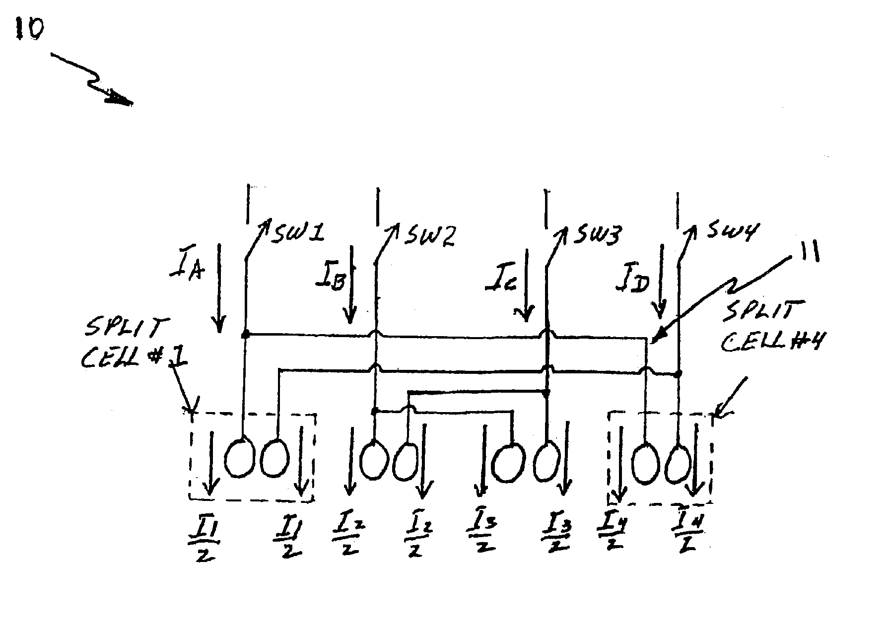
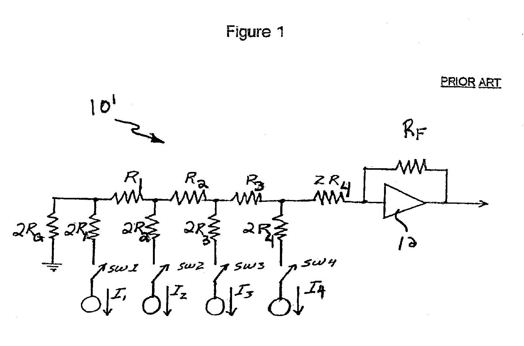
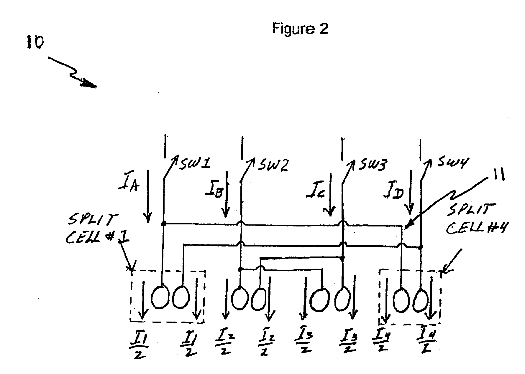
FIG. 1 shows an illustrative implementation of a four bit DAC in accordance with conventional teachings. The system 10′ has an operational amplifier 12 with a feedback resistor RF. Four current sources I1-I4 are selectively connected to the amplifier 12 by switches SW1-SW4 and resistors 2R1-2R4 respectively and resistors R1-R4. Ideally, each of the current sourc...


PUM


Abstract

A DAC (10) including an operational amplifier (12) having an input terminal; a plurality of current paths coupled to the input terminal; a plurality of current sources (I1 / 2 -I4 / 2); and an arrangement (11) for switchably coupling current from at least two of the cells to a respective one of the paths in response to an input signal. In a specific embodiment, the inventive DAC (10) further includes a first resistive element (2R1-2R4) disposed in each of the current paths, a second resistive element (R1-R4) disposed between the current paths, and a feedback resistor (RF) disposed between an output terminal of the amplifier and the input terminal thereof. In the illustrative embodiment, the coupling arrangement includes a plurality of switches (SW1-SW4); each of the switches is adapted to switch half of the current from a first source and half of the current from a second source into a respective one of the paths. The invention is adapted to lower the distortion of digital to analog converters by improving differential nonlinearities and integral nonlinearities, caused primarily by current source gradient errors, without the need for trimming.

Description

BACKGROUND OF THE INVENTION1. Field of the InventionThe present invention relates to electrical and electronic components, circuits and systems. More specifically, the present invention relates to digital to analog converters.2. Description of the Related ArtDigital to analog converters are widely used for converting digital signals to analog signals for many electronic circuits. For example, a high resolution, high speed digital to analog converter (DAC) may find application in video circuits, high quality audio, instrumentation applications, and in the transmit path for high dynamic range communications applications. DACs may also be used in high speed analog to digital converters (ADCs) such as successive approximation ADCs or subranging ADCs.As is known in the art, the function of an analog to digital converter (ADC) is to accurately convert an analog input signal into a digital output represented by a coded array of binary bits. The output bits are generated by processing the a...

Claims


Application Information

Patent Timeline
Patent Type & Authority Patents(United States)
IPC IPC(8): H03M1/06H03M1/74
CPCH03M1/0643H03M1/745
Inventor DEVENDORF, DON C.HIRATA, ERICK M.LINDER, LLOYD F.LANGIT, CHRISTOPHER B.KOSAKA, ROGER N.
Owner MICROELECTRONICS TECH INC
Why Eureka
Try Eureka