Eureka AIR delivers breakthrough ideas for toughest innovation challenges, trusted by R&D personnel around the world.

Broadband refractive objective for small spot optical metrology

a narrowband, optical metrology technology, applied in the field of optical metrology, can solve the problems of limiting the size of the focal spot, affecting the accuracy of the optical metrology, and becoming a source of measurement errors

Inactive Publication Date: 2005-04-12
THERMA WAVE INC
View PDF12 Cites 6 Cited by
  • Summary
  • Abstract
  • Description
  • Claims
  • Application Information

AI Technical Summary

Benefits of technology

[0017]The subject of this invention is a family of refractive optical lens designs for focusing broadband light. The lens consists of three elements made from at least two different optical materials arranged in two groups. The first group includes a positive lens and a negative lens (in the preferred embodiment these lenses are made from different optical materials) with net negative power. The second group consists of a single bi-convex lens (in the preferred embodiment this lens is made from the same material as the positive lens in the first group). The lens elements are specified according to a prescription where the lens faces are c

Problems solved by technology

Furthermore, reflective optics are more sensitive to manufacturing and alignment errors and, the polarization changes that occur upon reflection from the optical surfaces can become a source of measurement error in ellipsometric applications.
This design contains a central obscuration that blocks the light near zero numerical aperture and increases diffractive effects, limiting the size of the focal spot.
However, the only cost effective method for fabricating off-axis optical elements is diamond turning.
This characteristic error produced by diamond turning is one of the main factors limiting the spatial dimension over which accurate optical metrology measurements of a sample can be made.
Off-axis mirrors made with conventional polishing [e.g. the technique used to make some large astronomical telescopes] would have less scatter and therefore perform better; however the process is very expensive.
Replicated optics, characteristically molded in epoxy using a precision form, can be made cost-effectively; however, the performance and durability of these mirrors in optical metrology applications remain unproven.
Off-axis spherical mirror systems can be made with no central obscuration and can be finished by conventional polishing techniques; however, an off-axis spherical mirror can generate significant amounts of geometrical aberrations which enlarge the resultant focal spot.
This design form is highly stressed and is sensitive to manufacturing and alignment errors.
However, because the refractive index of virtually all materials is wavelength dependent, refractive lenses exhibit chromatic aberration.
It is difficult to develop broadband lens designs that are corrected for chromatic aberration over large spectral bandwidths.
It is extremely difficult to develop large bandwidth, chromatically corrected designs that meet the requirements of small-spot optical wafer metrology systems.
However, the design is not appropriate for small-spot optical metrology where axial spot size over all wavelengths must be carefully controlled.
The microscope objective is designed to produce small-spot illumination; however, since both first and second lens groups have positive power the chromatic aberration of the objective is difficult to minimize.
Consequently, the objective is not suitable for small-spot, broadband wafer metrology applications.
Further, these designs are unable to achieve the balance of axial spot over all wavelengths without an unacceptable level of sensitivity to misalignment or fabrication errors, or without adding more elements, which make them both more expensive, and also more prone to birefringence problems, which make them inappropriate for ellipsometric applications.
None of the prior art reflective, catadioptric and refractive designs are entirely satisfactory.

Method used


Image

  • Broadband refractive objective for small spot optical metrology
  • Broadband refractive objective for small spot optical metrology
  • Broadband refractive objective for small spot optical metrology

Examples


example 1

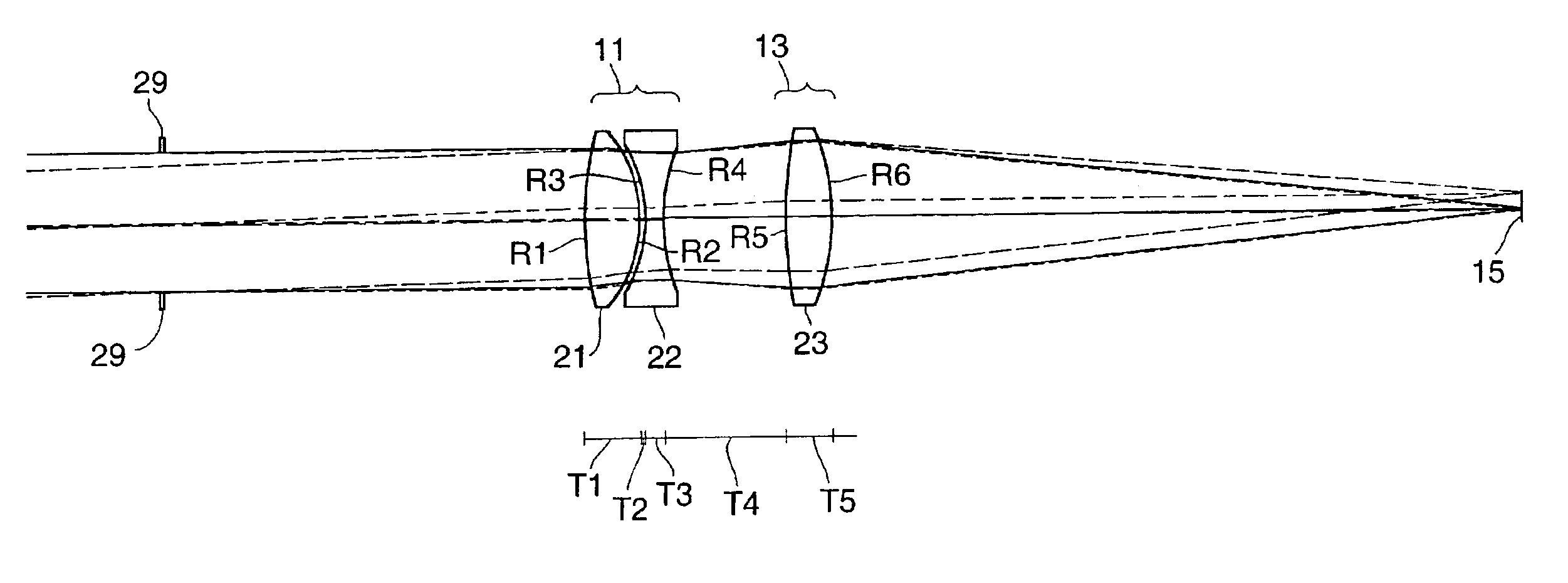
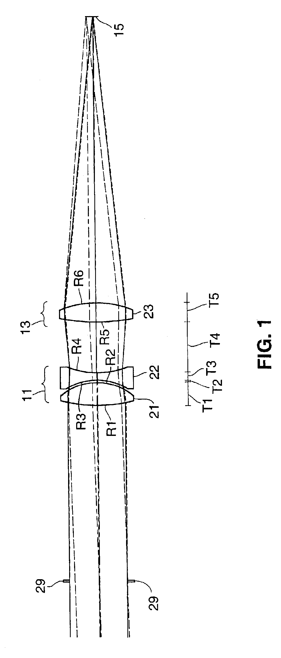
r1 = 0.481Ft1 = 0.083Fr2 = −0.231Ft2 = 0.008Fr3 = −0.218Ft3 = 0.025Fr4 = 0.314Ft4 = 0.185Fr5 = 0.970Ft5 = 0.066Fr6 = −0.392F

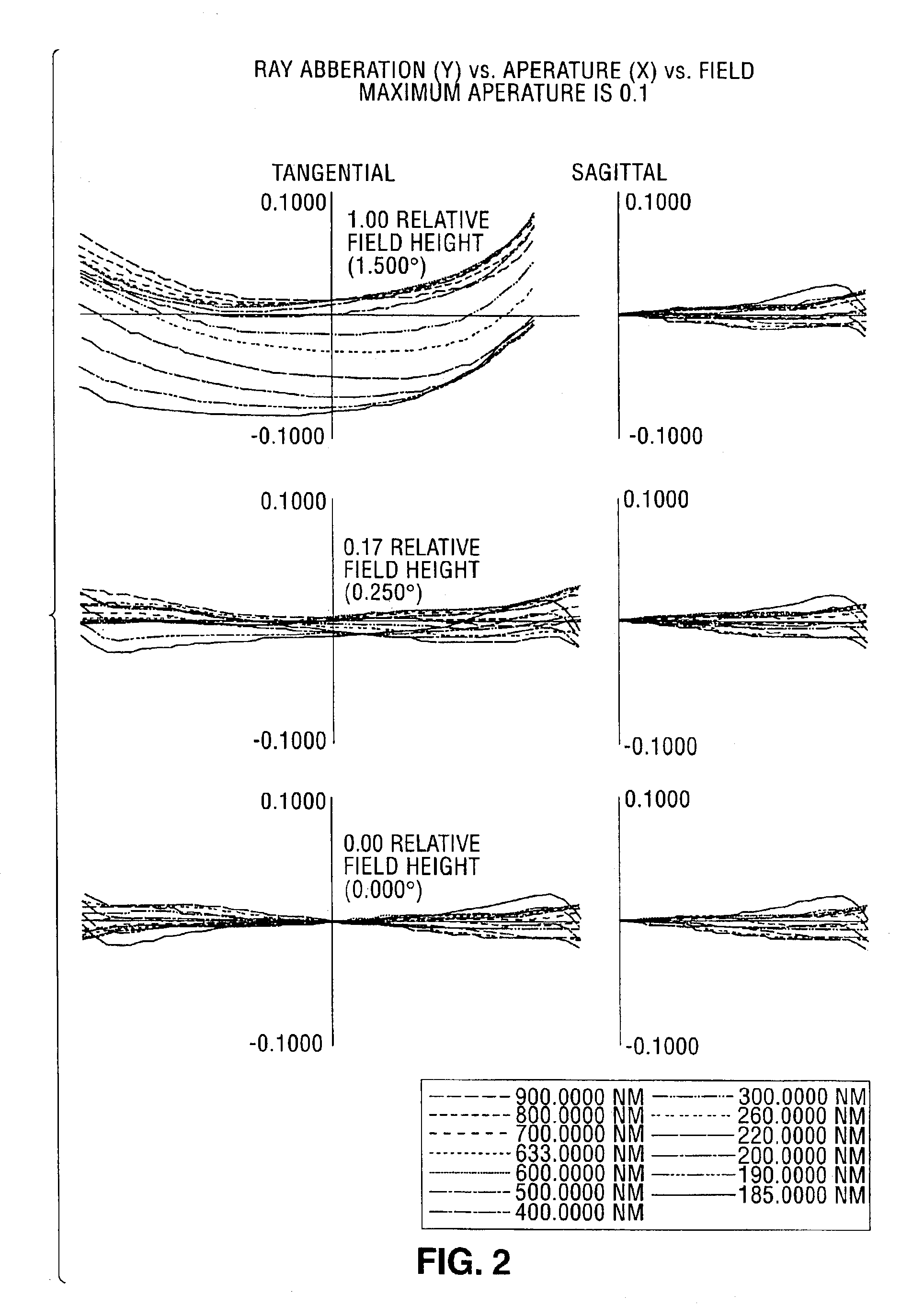
[0029]FIG. 2 shows transverse aberration plots for the preferred embodiment illustrated in FIG. 1. A total of six plots are shown. The plots are grouped in pairs and arranged vertically. For each pair the plot on the left corresponds to y-directed (tangential) ray intercept errors (mm) vs. relative NA, and the plot on the right shows the corresponding x-directed (sagittal) errors (mm) vs. relative NA. Calculations were performed for several discrete wavelengths spanning the spectral region between 185 and 900 nm. The NA varies between 0 and 0.1.

[0030]The lower two plots correspond to the on-axis aberrations. The on axis errors are small, significantly less than ±0.03 mm for relative 0≦NA≦0.1. Furthermore, the wavelength dependence of the aberrations is weak. In the spectroscopic ellipsometers manufactured by the assignee herein, these on-axis curves correspond ...

example 2

r1 = 0.741Ft1 = 0.091Fr2 = −0.263Ft2 = 0.015Fr3 = −0.247Ft3 = 0.036Fr4 = 0.281Ft4 = 0.088Fr5 = 0.530Ft5 = 0.082Fr6 = −0.366F

[0036]The refractive objective may be employed as part of the illumination system and / or part of the light collection system in optical metrology applications. In general, the refractive objective may be used as a substitute for any off-axis focusing mirror in collimated space. Consequently, the refractive objective is applicable to the design of the majority of broadband optical metrology tools including spectroscopic reflectometers, spectroscopic ellipsometers, spectroscopic scatterometers and optical CD metrology tools.

[0037]When used in an illumination system, the refractive objective is situated between the light source and the sample. In one arrangement, the refractive objective brings the source light to a sharp focus at a desired location for purpose of spatial filtering. In another arrangement, the refractive objective collimates the source beam, for r...


PUM


Abstract

The subject invention relates to broadband optical metrology tools for performing measurements of patterned thin films on semiconductor integrated circuits. Particularly a family of optical designs for broadband, multi-wavelength, DUV-IR (185<λ<900 nm) all-refractive optical systems. The designs have net focusing power and this is achieved by combining at least one positively powered optical element with one negatively powered optical element. The designs have small spot-size over the wavelength range spanning 185-900 nm with substantially reduced spherical aberration, axial color, sphero-chromatism and zonal spherical aberration. The refractive optical systems are broadly applicable to a large class of broadband optical wafer metrology tools including spectrophotometers, spectroscopic reflectometers, spectroscopic ellipsometers and spectroscopic scatterometers.

Description

PRIORITY CLAIM[0002]This application is a continuation of U.S. application Ser. No. 10 / 222,296, filed Aug. 16, 2002 now U.S. Pat. No. 6,587,250, which also claims priority to U.S. Provisional Patent Application Nos. 60 / 316,191, filed Aug. 30, 2001, and 60 / 330,255, filed Oct. 15, 2001.TECHNICAL FIELD[0003]The subject invention relates to the field of optical metrology, particularly broadband optical metrology tools for performing measurements of patterned thin films on semiconductor integrated circuits.BACKGROUND OF THE INVENTION[0004]A number of metrology tools are now available for performing optical measurements on semiconductors. Such tools can include spectrophotometers, spectroscopic reflectometers, spectroscopic ellipsometers and spectroscopic scatterometers. Examples of such tools can be found in U.S. Pat. Nos. 5,608,526 and 6,278,519, both incorporated by reference. Such tools typically include a broadband light source for generating a probe beam that is directed to reflect ...

Claims


Application Information

Patent Timeline
IPC IPC(8): G02B13/14G02B9/12G02B9/14G02B9/16
CPCG02B9/14G02B13/146G02B9/16
Inventor WANG, DAVID Y.AIKENS, DAVID M.
Owner THERMA WAVE INC
Why Eureka
Eureka Blog
Learn More