Method for fabricating a structure for making contact with an IC device

a technology of ic devices and structures, applied in the field of probe structures, can solve the problems of limiting the substrate used for fabrication of this probe fixture to semiconductor wafers which are relatively expensive, rigid and do not provide a wiping interface with the mating contacts, and the potential for etc., to achieve the effect of high density and minimal damage to the interconnect circuit wiring

Inactive Publication Date: 2005-04-19
TOKYO ELECTRON LTD
View PDF3 Cites 4 Cited by
  • Summary
  • Abstract
  • Description
  • Claims
  • Application Information

AI Technical Summary

Benefits of technology

[0012]Another object of the present invention is to provide a probe structure that is an integral part of the fan out wiring on the test substrate or other printed wiring means to minimize the electrical conductor length as well as the contact resistance of the probe interface.
[0015]Yet another object of the present invention is to provide a fabrication process that minimizes the potential for damaging the interconnect circuit wiring in the substrate material.
[0016]Yet an additional object of the present invention is to provide a high density probe structure to allow multiple chips to be tested by a single test fixture.

Problems solved by technology

Although this technique is similar to the probe structure described in this patent application, it is limited to substrates made from a silicon wafer or other semiconductor materials.
The probes described in this patent are rigid and do not provide a wiping interface with the mating contacts on the IC device.
Also, the substrate used for fabrication of this probe fixture is limited to semiconductor wafers which are relatively expensive.
High temperature applications of this type of probe are limited due to the glass transition temperature of the polymer material surrounding the probes as well as the coefficient of thermal expansion mismatch between the compliant polymer material and the rigid substrate.

Method used


Image

  • Method for fabricating a structure for making contact with an IC device
  • Method for fabricating a structure for making contact with an IC device
  • Method for fabricating a structure for making contact with an IC device

Examples


embodiment

Preferred Embodiment

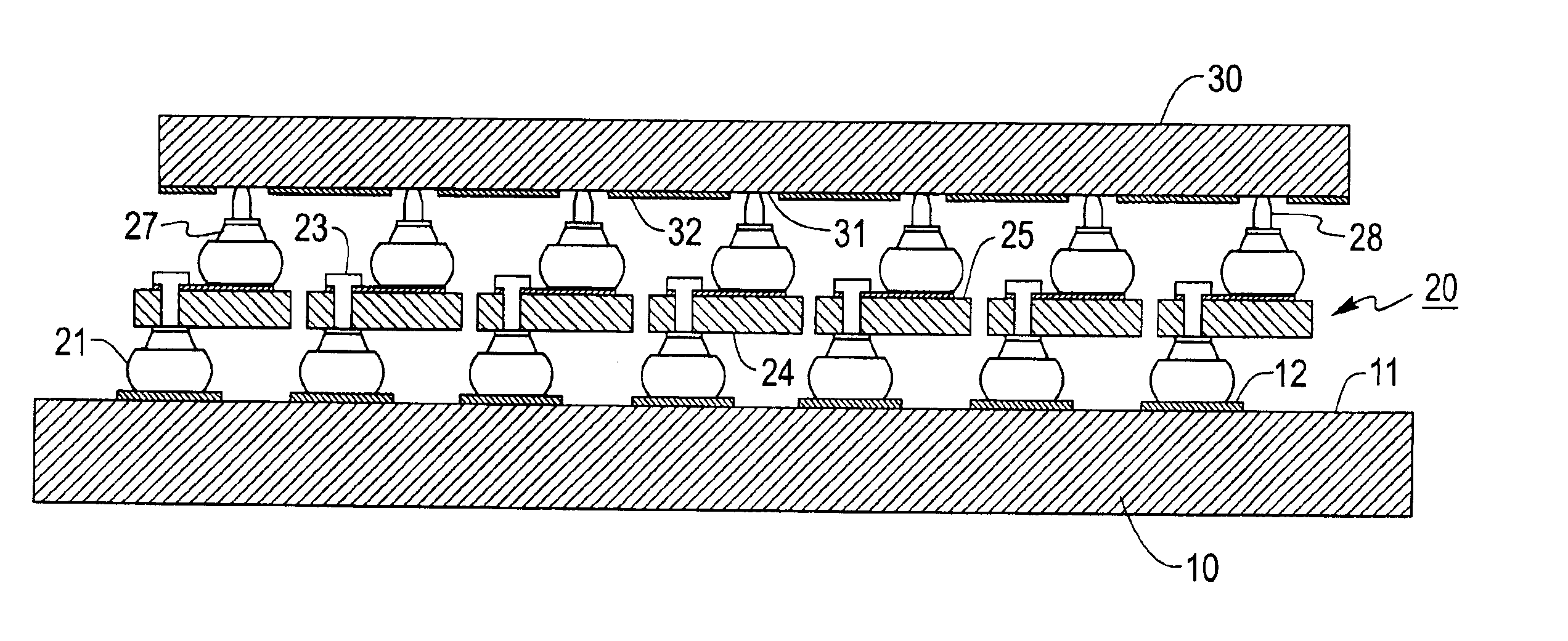
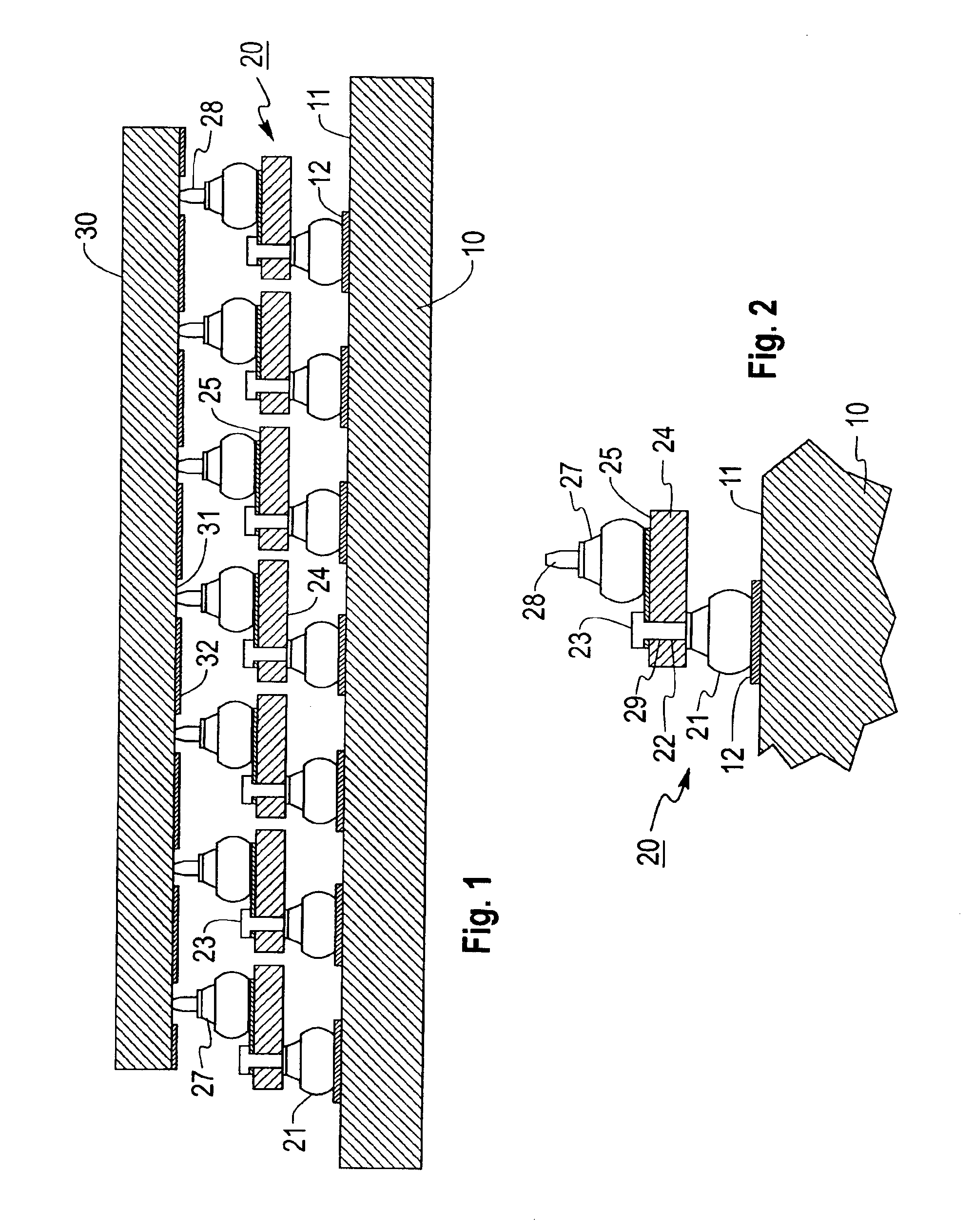
[0026]FIG. 1 shows a cross section of a test substrate (10) and high density cantilever test probe (20) according to the present invention. The test substrate (10) provides a rigid base for attachment of the probe structures (20) and fan out wiring from the high density array of probe contacts to a larger grid of pins or other interconnection means to the equipment used to electrically test the integrated circuit device. The fan out substrate can be made from various materials and constructions including single and multi-layer ceramic with thick or thin wiring, silicon wafer with thin film wiring, or epoxy glass laminate construction with high density copper wiring. The cantilever test probes (20) are attached to the first surface (11) of the substrate (10). The probes are used to contact the bond pads (31) on the integrated circuit device (30). The surface of the bond pads (31) are recessed slightly below the surface of the passivation layer (32) on the integrat...


PUM

PropertyMeasurementUnit
flexibleaaaaaaaaaa
densityaaaaaaaaaa
temperatureaaaaaaaaaa

Abstract

Probes for electronic devices are described. The probe is formed by ball bonding a plurality of wires to contact locations on a fan out substrate surface. The wires are cut off leaving stubs. A patterned polymer sheet having electrical conductor patterns therein is disposed over the stubs which extend through holes in the sheet. The ends of the wires are flattened to remit the polymer sheet in place. The wire is connected to an electrical conductor on the polymer sheet which is converted to a contact pad on the polymer sheet. A second wire is ball bonded to the pad on the polymer sheet and cut to leave a second stub. The polymer sheet is laser cut so that each second stub is free to move independently of the other second studs. The ends of the second stubs are disposed against contact locations of an electronic device, such as an FC chip, to test the electronic device.

Description

[0001]The present application is a division of application Ser. No. 09 / 928,285, filed on Aug. 10, 2001, now U.S. Pat. No. 6,722,032, which is a CON of Ser. No. 09 / 208,529, filed on Dec. 9, 1998, now U.S. Pat. No. 6,329,827, which is a DIV of Ser. No. 08 / 946,141, filed on Oct. 7, 1997, now U.S. Pat. No. 5,914,614, which is a DIV of Ser. No. 08 / 614,417, filed on Mar. 12, 1996, now U.S. Pat. No. 5,811,982.FIELD OF THE INVENTION[0002]The present invention is directed to probe structures for testing of electrical interconnections to integrated circuit devices and other electronic components and particularly to testing integrated circuit devices with flat or recessed surfaces for wired bonded interconnections.BACKGROUND OF THE INVENTION[0003]Integrated circuit (IC) devices and other electronic components are normally tested to verify the electrical function of the device and certain devices require high temperature burn-in testing to accelerate early life failures of these devices. The va...

Claims


Application Information

Patent Timeline
Patent Type & Authority Patents(United States)
IPC IPC(8): G01R1/067G01R3/00G01R1/073H05K3/32H05K3/40G01R31/28
CPCG01R1/06711G01R3/00G01R31/2886H05K3/326H05K3/4015G01R1/07307G01R1/06727Y10T29/49218G01R1/07342H01L2224/1134H05K1/118H05K3/328H05K2201/09081H05K2203/049H01L2924/00013Y10T29/49155Y10T29/49124Y10T29/49204Y10T29/49147Y10T29/49815Y10T29/49004Y10T29/49208Y10T29/49149Y10T29/49222Y10T29/49144H01L2224/13099H01L2224/05571H01L2224/05573H01L2924/00014H01L2224/05599
Inventor BEAMAN, BRIAN SAMUELFOGEL, KEITH EDWARDLAURO, PAUL ALFREDNORCOTT, MAURICE HEATHCOTESHIH, DA-YUAN
Owner TOKYO ELECTRON LTD
Why Eureka
Try Eureka