Solder bump structure and laser repair process for memory device

a memory device and laser repair technology, applied in the direction of light-sensitive devices, basic electric elements, electrolytic capacitors, etc., can solve the problems of oxidation of the probing mark on the surface of the bump pad b>14/b>, difficult problems, bare copper or crack insulation layers, etc., to prevent the formation of voids

Inactive Publication Date: 2005-04-19
UNITED MICROELECTRONICS CORP
View PDF9 Cites 22 Cited by
  • Summary
  • Abstract
  • Description
  • Claims
  • Application Information

AI Technical Summary

Benefits of technology

[0012]The solder bump structure and laser repair process for memory device according to the claimed invention comprise first performing an UBM process and forming a solder bump, and then performing a circuit probing process through the solder bump. Finally, the laser repair process is performed. Therefore, the quality of the metal layer formed on a surface of the bump pad and the structure of electronic devices on the semiconductor wafer avoid being damaged by the circuit probing process. Additionally, the claimed invention also prevents the formation of the voids in the second dielectric layer, which affects the reliability of products.

Problems solved by technology

The prior art method causes several problems as a result of performing the circuit probing and laser repair process before forming the second dielectric layer 22 and the metal layer 24.
Additionally, when an interconnect system uses a cooper process and low-k materials as insulation layers, the circuit probing process directly performed on the bump pad 14 may result in bare copper or crack insulation layers because of excess probing force.
As well, oxidation of the probing mark on the surface of the bump pad 14 is a difficult problem.

Method used


Image

  • Solder bump structure and laser repair process for memory device
  • Solder bump structure and laser repair process for memory device
  • Solder bump structure and laser repair process for memory device

Examples


Embodiment Construction

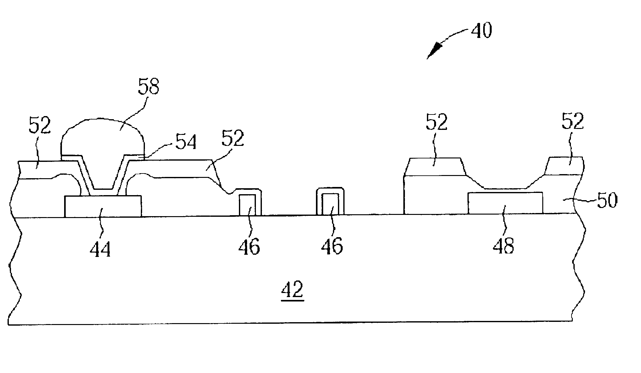
[0017]Please refer to FIG. 5 to FIG. 7 of schematic views of forming a solder structure and performing a laser repair process for memory device on a semiconductor wafer 40 according to a first embodiment of the present invention. As shown in FIG. 5, the semiconductor wafer 40 comprises a substrate 42, which has an integrated circuit region (not shown) comprising an embedded memory array formed on its surface. The surface of the substrate 42 further comprises a bump pad 44, a plurality of fuses 46, and an alignment key 48, and a silicon oxide layer (not shown) is formed on surfaces of the fuses 46 and the alignment key 48. The bump pad 44 is electrically connected with the integrated circuit region. Therefore, after completing a subsequent packaging process, the integrated circuit is able to electrically connect to an external circuit through the bump pad 44. The fuses 46 are formed on an upper layer of the integrated circuit region and electrically connected with the embedded memory...


PUM


Abstract

A solder bump structure and laser repair process for memory device include forming a first dielectric layer on a bump pad of a semiconductor wafer. After that, the first dielectric layer is etched to form a contact hole and to expose portions of the bump pad. A second dielectric layer is then formed on a surface of the semiconductor wafer outside of the contact hole. An under bump metallurgy (UBM) process is performed to form a metal layer on a surface of the contact hole, and a solder bump is formed on the metal layer. Finally, the laser repair process for memory device is completed.

Description

BACKGROUND OF INVENTION[0001]1. Field of the Invention[0002]The present invention relates to a process of performing a laser repair process for memory device after formation of a solder bump.[0003]2. Description of the Prior Art[0004]High performance microelectronic devices often use solder balls or solder bumps for electrical and mechanical interconnection to other microelectronic devices. For instance, an ultra large scale integration (ULSI) chip may be electrically connected to a circuit board or other second stage packaging substrate by using solder balls or solder bumps. This connection technology is also referred to as “Flip-chip packaging, FC” technology.[0005]Please refer to FIG. 1 to FIG. 4 of schematic views of performing a laser repair process for memory device on a semiconductor wafer 10 according to a prior art method. As shown in FIG. 1, the semiconductor wafer 10 comprises a substrate 12, which has an integrated circuit region (not shown) comprising an embedded memory...

Claims


Application Information

Patent Timeline
Patent Type & Authority Patents(United States)
IPC IPC(8): H01L21/20H01L21/4763H01L21/44H01L21/02H01L21/60H01L21/768H01L23/485H01L23/525H01L23/544
CPCH01L21/76894H01L24/11H01L2224/05572H01L23/544H01L24/02H01L2224/13099H01L2924/01029H01L2924/01078H01L2924/14H01L2224/0401H01L2924/01019H01L2924/01033H01L2924/014H01L2924/0002H01L23/5256H01L2924/00014H01L2224/05552H01L2924/12042H01L2224/13022H01L24/03H01L24/05H01L24/13H01L2924/00
Inventor CHEN, KUO-MINGLIU, HUNG-MIN
Owner UNITED MICROELECTRONICS CORP
Why Eureka
Try Eureka