Ball grid array resistor network having a ground plane

a grid array resistor and ground plane technology, applied in resistor details, resistor mounting/supporting, printed resistor incorporation, etc., can solve the problems of difficult to achieve a well matched impedance value in present resistor networks, coupled electrical energy may be coupled between adjacent conductors, etc., to achieve low coupled noise

Inactive Publication Date: 2005-04-19
CTS CORP ELKHART
View PDF17 Cites 17 Cited by
  • Summary
  • Abstract
  • Description
  • Claims
  • Application Information

AI Technical Summary

Benefits of technology

[0013]It is a feature of the invention to provide a ball grid array resistor network that has low coupled noise.

Problems solved by technology

One problem that can occur in electronic packages is that electromagnetic energy may be coupled between adjacent conductors such as circuit lines.
Due to space constraints and the dielectric constants of the substrate materials used, it is difficult to achieve a well matched impedance value in present resistor networks.

Method used


Image

  • Ball grid array resistor network having a ground plane
  • Ball grid array resistor network having a ground plane
  • Ball grid array resistor network having a ground plane

Examples


Embodiment Construction

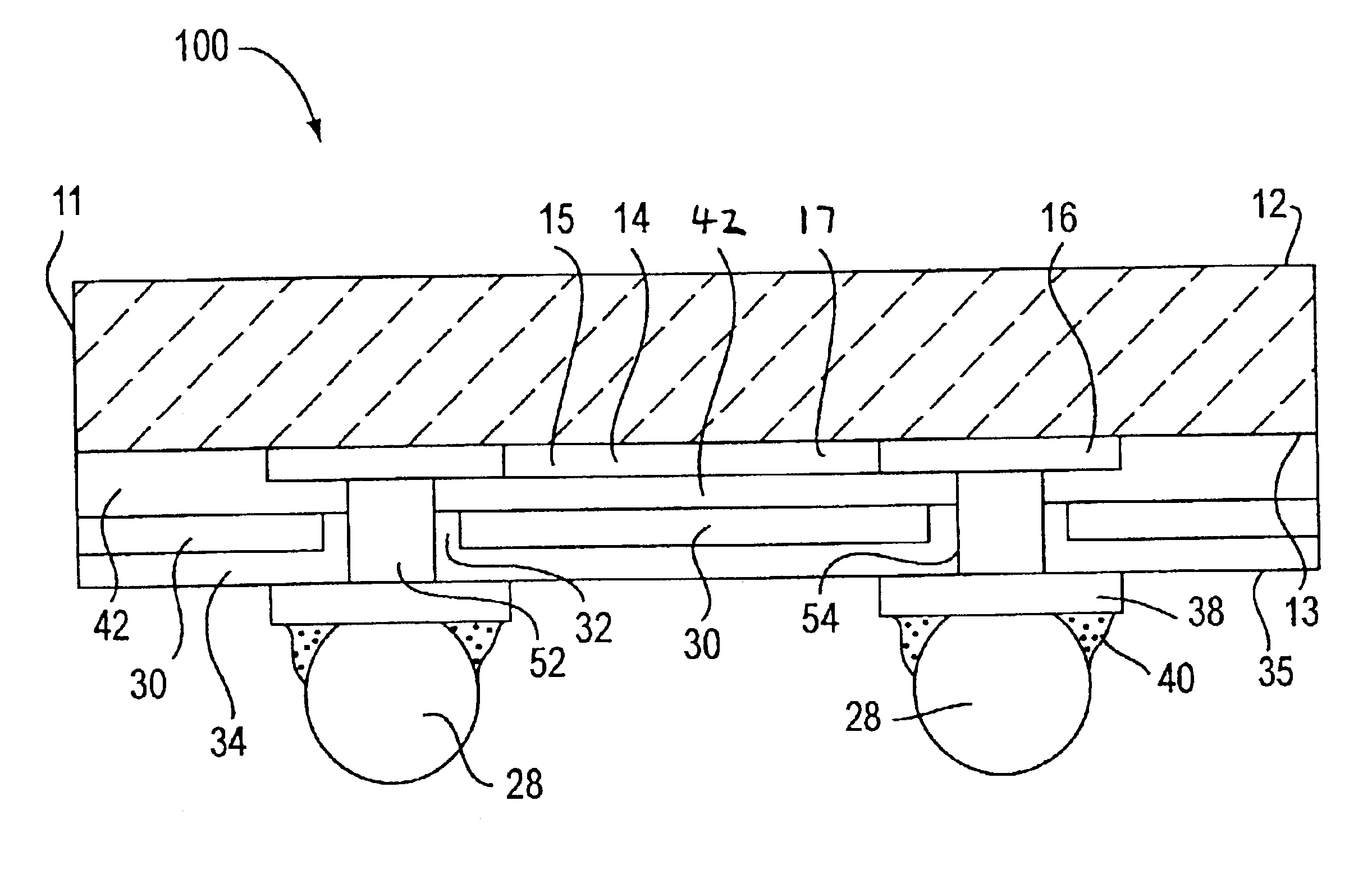
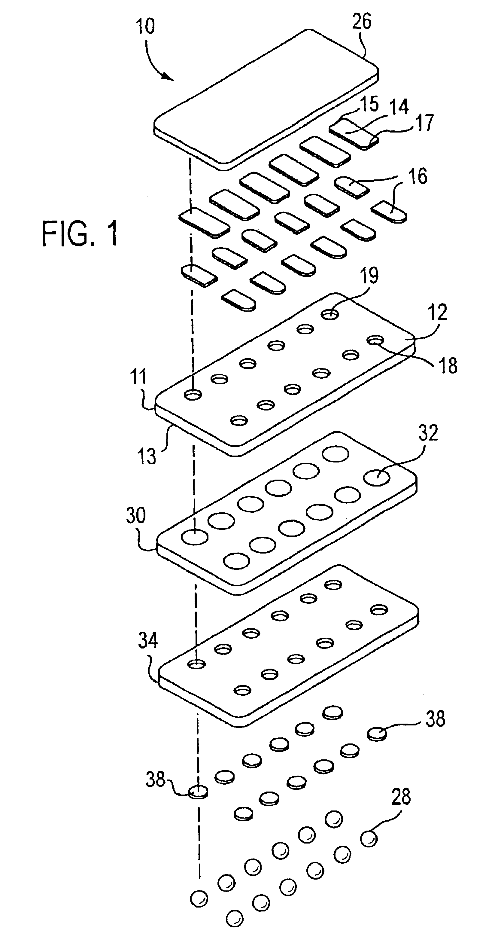
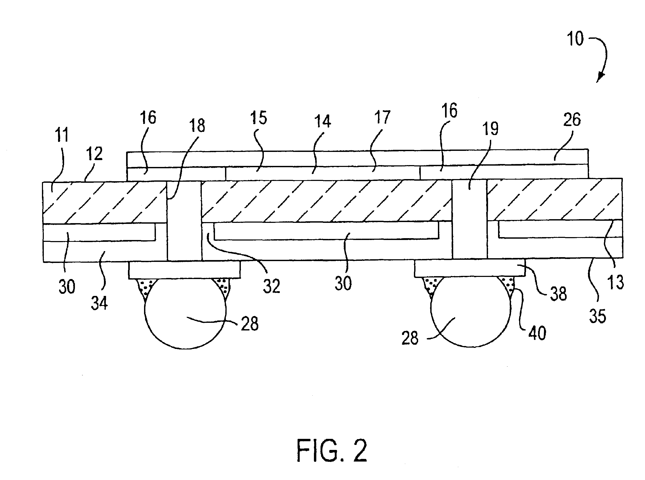
[0019]Referring to FIGS. 1 and 2, there is a ball grid array resistor network assembly 10. In particular, resistor network assembly 10 has a planar substrate 11 having a top surface 12 and a bottom surface 13. Substrate 11 is preferably made out of a ceramic material such as alumina oxide. Substrate 11 has holes or vias 18 that are formed prior to firing the alumina ceramic. Resistors 14 are disposed and trimmed on the top surface 12 by conventional thick film resistor processing techniques. These techniques are detailed in U.S. Pat. No. 6,326,677, which is herein incorporated by reference.

[0020]Resistors 14 have a first end 15 and a second end 17. Conductors 16 are disposed on the top surface 12 by conventional thick film conductor processing techniques. Conductors 16 are placed on each end 15 and 17 of resistors 14 and are electrically connected to ends 15 and 17. Conductors 16 and resistors 14 slightly overlap and sinter to form a mechanical and electrical bond during processing....


PUM


Abstract

A ball grid array resistor network that has a ground plane to reduce noise and improve signal integrity. The ball grid array resistor network includes a substrate having a first and a second surface and vias that extending through the substrate between the first and second surfaces. Resistors are located on the first surface between the vias. Conductors are located over the vias and are electrically connected to ends of the resistors. A cover coat covers the conductors and resistors. A ground plane is located on the second surface. An insulating layer is located over the ground plane. Ball pads are located over the vias. The ball pads are electrically connected to the vias. Solder spheres are attached to the ball pads.

Description

CROSS REFERENCE TO RELATED APPLICATIONS[0001]The present application is related to U.S. Pat. No. 6,326,677.BACKGROUND[0002]1. Field of the Invention[0003]This invention generally relates to shielding of a dense package in a high frequency environment. The invention further relates to isolation and impedance matching for electronics. Specifically, the invention is a group of resistors mounted in a high density network or array package with a ground plane that uses solder balls to connect with a circuit board.[0004]2. Description of the Related Art[0005]Resistor networks are commonly used to terminate high speed digital signal lines to minimize unwanted reflections back through the transmission structure by matching the impedance of the transmission structure. In most applications, the terminations are made by placing a resistor matching the impedance of the transmission line at the end of the transmission line. One end of the resistor is connected to a common termination voltage and ...

Claims


Application Information

Patent Timeline
Patent Type & Authority Patents(United States)
IPC IPC(8): H01C1/144H01C1/00H01C1/16H01C1/14H01L23/498H01L23/48H05K3/34H05K1/16
CPCH01C1/144H01C1/16H01L23/49816H05K1/167H01L2924/0002H05K3/3436H01L2924/00
Inventor CHRISTIAN, DAVID A.CHRISTIAN, CYNTHIA A.COOPER, RICHARDTU, YINGGANG
Owner CTS CORP ELKHART
Why Eureka
Try Eureka