Focus masking structures, focus patterns and measurements thereof

a technology of focus masking and focus pattern, applied in the field of photolithography methods and systems, can solve the problems of misfocus found between the surface of the wafer, adversely affecting the printed pattern on the wafer, and causing one portion of the chip to run faster or slower

Inactive Publication Date: 2005-04-26
KLA TENCOR TECH CORP
View PDF22 Cites 35 Cited by
  • Summary
  • Abstract
  • Description
  • Claims
  • Application Information

AI Technical Summary

Benefits of technology

[0007]The invention relates, in one embodiment, to a focus masking structure used to determine the focus quality of a photolithographic pattern or a photolithographic system. The focus masking structure is generally disposed on a substrate. The focus masking structure includes a plurality of parallel source lines. The focus masking structure also includes a plurality of phase shift zones configured to separate the plurality of parallel source lines. The plurality of phase shift zones alternate between a first phase shift zone and a second phase shift zone. In one implementation, the first and second phase shift zones have phases that are not equal to the phase of the substrate, and a phase difference therebetween that is not equal to 0 or 180 degrees or integer multiples of 180 degrees. Furthermore, the plurality of parallel source lines and phase shift zones cooperate to produce a focus pattern that includes at least two periodic structures that shift relative to one another with changes in focus. In most cases, the shifts are based on the sign and magnitude of defocus.
[0008]The invention relates, in another embodiment, to a focus pattern used to determine the focus quality of a photolithographic pattern or a photolithographic system. The focus pattern is generally disposed on a surface of a workpiece such as a wafer. The focus pattern is generally produced by a focus masking structure. The focus pattern includes a first periodic structure having a plurality of parallel first printed lines. Each of the first printed lines are formed by a first phase transition of the focus masking structure. The focus pattern also includes a second periodic structure having a plurality of parallel second printed lines. Each of the second printed lines are formed by a second phase transition of the focus masking structure. The second phase transition is different than the first phase transition. Furthermore, the first and second periodic structures form measurable shifts therebetween that correspond to system defocus. In most cases, the measurable shifts are based on the sign and magnitude of defocus.
[0009]The invention relates, in another embodiment, to a method of determining the focus quality of a photolithographic pattern or a photolithographic system. The method includes providing a focus masking structure configured to produce a focus pattern. The focus masking structure generally includes a plurality of source lines that are separated by alternating phase shift zones. The method further includes forming a focus pattern on a work piece with the focus masking structure. The focus pattern generally includes a plurality of periodic structures that form measurable shifts therebetween corresponding to the sign and magnitude of defocus. The method also includes obtaining focus information from the focus pattern. The focus information is based at least in part on the measurable shifts between the plurality of periodic structures.

Problems solved by technology

One problem that has been encountered during lithographic processes is the misfocus found between the surface of the wafer being patterned on and the ideal focus plane.
That is, there is Z axis displacement between the ideal focus plane and the surface of the wafer being written on and thus there is misfocus.
Unfortunately, misfocus may adversely effect the printed pattern on the wafer.
The linewidth generally determines the speed and the timing across the circuit and thus misfocus may cause one portion of the chip to run faster or slower than another portion of the chip.
In addition, misfocus may cause open or shorted circuits such that the chip must be discarded or reworked.

Method used


Image

  • Focus masking structures, focus patterns and measurements thereof
  • Focus masking structures, focus patterns and measurements thereof
  • Focus masking structures, focus patterns and measurements thereof

Examples


Embodiment Construction

[0032]The present invention will now be described in detail with reference to a few preferred embodiments thereof as illustrated in the accompanying drawings. In the following description, numerous specific details are set forth in order to provide a thorough understanding of the present invention. It will be apparent, however, to one skilled in the art, that the present invention may be practiced without some or all of these specific details. In other instances, well known process steps have not been described in detail in order not to unnecessarily obscure the present invention.

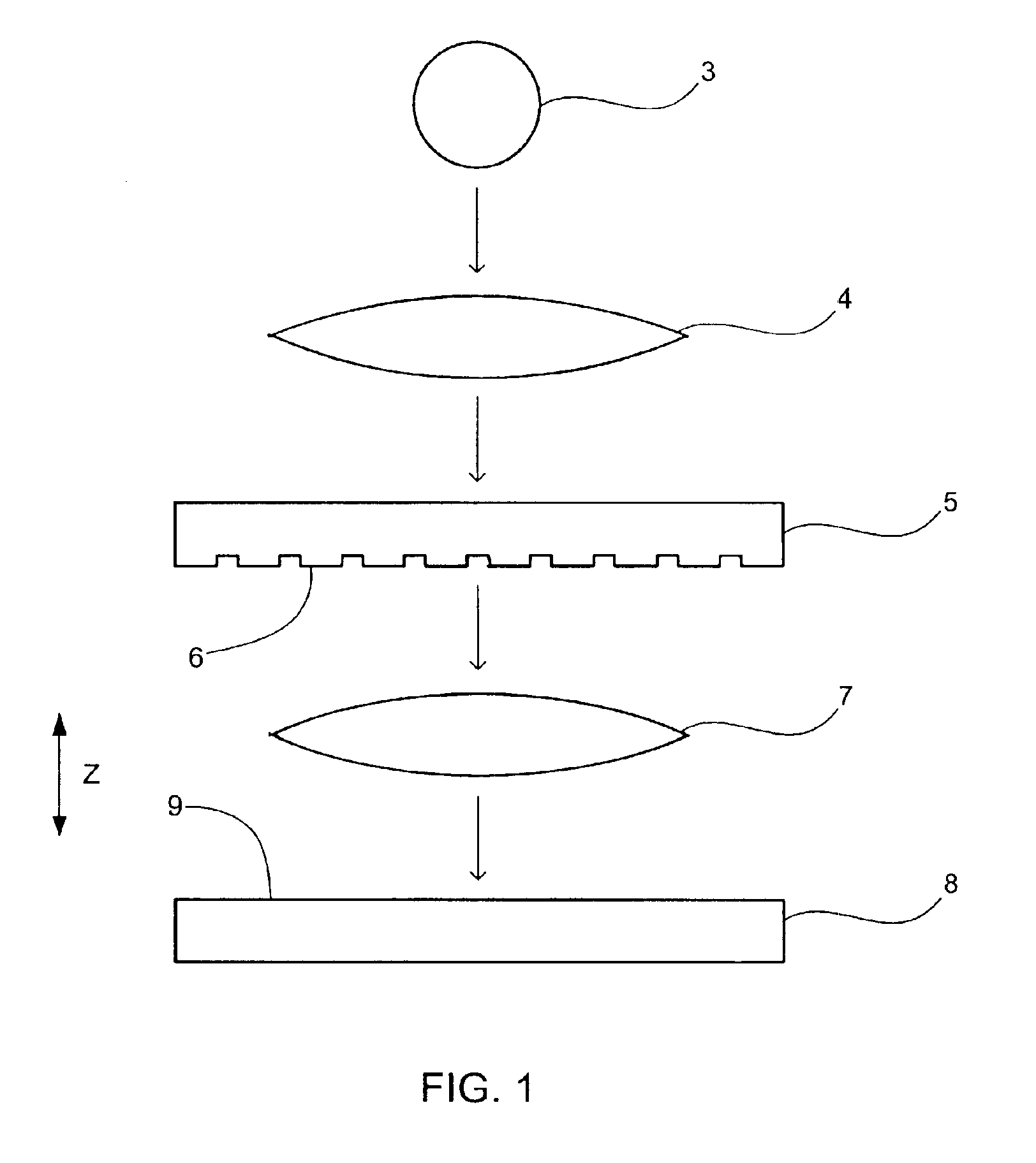
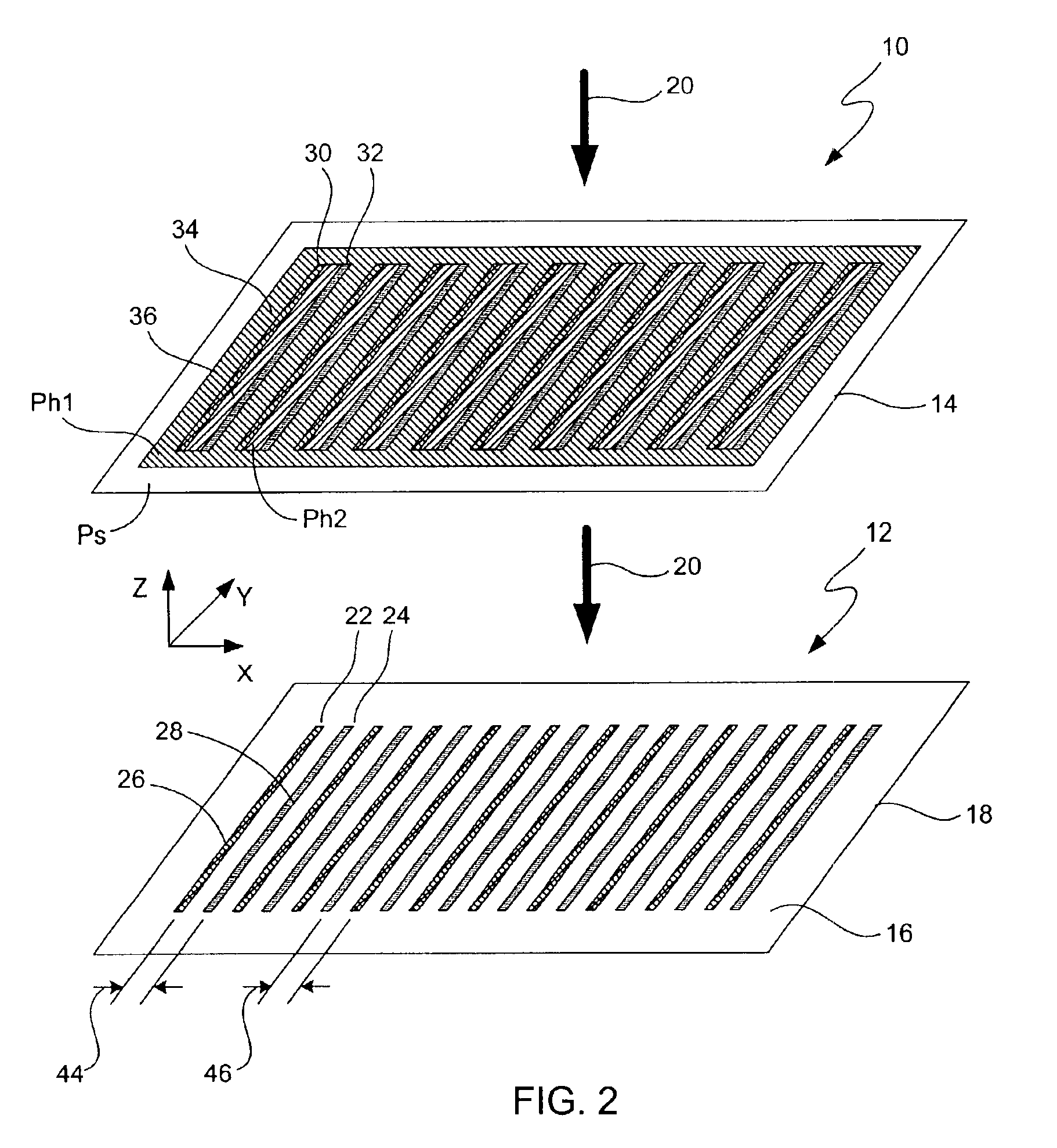
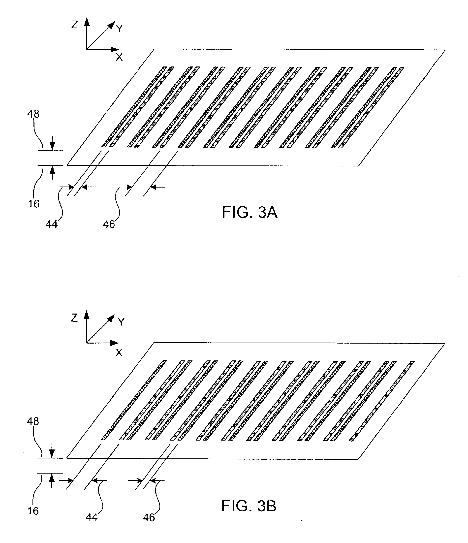
[0033]FIG. 2 is a simplified perspective view of a focus masking structure 10, in accordance with one embodiment of the present invention. The focus masking structure 10 is generally provided to produce a focus pattern 12 corresponding to the focus quality of a photolithographic pattern or a photolithographic system. The focus pattern 12 may be used to improve the focus control of subsequent lithographic pa...


PUM

PropertyMeasurementUnit
widthsaaaaaaaaaa
widthsaaaaaaaaaa
phaseaaaaaaaaaa

Abstract

Methods and device structures used to determine the focus quality of a photolithographic pattern or a photolithographic system are disclosed. One aspect of the invention relates to focus masking structures configured to form focus patterns that contain focus information relating to the focus quality. The focus masking structures generally include a plurality of parallel source lines that are separated by alternating phase shift zones. Another aspect of the invention relates to focus patterns that change with changes in focus. The focus patterns generally include a plurality of periodic structures that form measurable shifts therebetween corresponding to the sign and magnitude of defocus. Another aspect of the invention relates to a method of determining the focus quality of a photolithographic pattern or a photolithographic system. The method generally includes: providing a focus masking structure, forming a focus pattern on a work piece with the focus masking structure, and obtaining focus information from the focus pattern. The focus information may be obtained using a variety of techniques, as for example, scatterometry techniques, scanning techniques, imaging techniques, phase based techniques, and the like.

Description

CROSS REFERENCE TO RELATED APPLICATION[0001]This application claims the priority of U.S. Provisional No. 60 / 338,204, filed on Nov. 9, 2001, which is hereby incorporated by reference.BACKGROUND OF THE INVENTION[0002]The present invention relates generally to photolithography methods and systems, and more specifically to improved techniques for determining focus error.[0003]Integrated circuits are made by photolithographic processes, which use photolithographic masks and an associated light or radiation source to project a circuit image onto a wafer. Referring to FIG. 1, for example, a simplified diagram of a lithography system 2 is shown. By way of example, the lithography system may correspond to a stepper or scanning system. The lithography system 1 typically includes a light or radiation source 3 and a first set of optics 4 that illuminate a mask 5 having a circuit pattern 6 disposed thereon. In order to form the circuit pattern, the mask 6 may include opaque portions and / or trans...

Claims


Application Information

Patent Timeline
Patent Type & Authority Patents(United States)
IPC IPC(8): G03F7/20G02B7/28G03F1/28G03F7/207H01L21/027
CPCG06K7/0095G03F7/70641G03F1/28G03F1/44
Inventor MIEHER, WALTER DEANWACK, DANIELLEVY, ADY
Owner KLA TENCOR TECH CORP
Why Eureka
Try Eureka