Method for depositing a coating having a relatively high dielectric constant onto a substrate

a technology of dielectric constant and substrate, which is applied in the direction of chemical vapor deposition coating, solid-state diffusion coating, coating, etc., can solve the problems of limiting the performance of the resulting electronic device, adversely degrading with the overall performance of the electrical device, and a wide range of properties

Inactive Publication Date: 2005-04-26
RGT UNIV OF CALIFORNIA +1
View PDF40 Cites 104 Cited by
  • Summary
  • Abstract
  • Description
  • Claims
  • Application Information

AI Technical Summary

Problems solved by technology

However, chemical vapor deposition generally results in relatively thick layers that have a number of defects, which can limit the performance of the resulting electronic devices.
However, such high temperatures can sometimes cause unwanted crystallization of the coating, further increasing the leakage current through the grain boundaries, which can adversely degrade with the overall performance of the electrical device.
Although atomic layer deposition has some benefits over prior methods, it also possesses a variety of problems.
For example, atomic layer deposition provides for very little processing control and, as a result, certain target characteristics of the dielectric coating may not be readily achieved.
In addition, because atomic layer deposition is limited to one monolayer per reaction cycle, its effectiveness in a production environment may be limited.

Method used


Image

  • Method for depositing a coating having a relatively high dielectric constant onto a substrate
  • Method for depositing a coating having a relatively high dielectric constant onto a substrate
  • Method for depositing a coating having a relatively high dielectric constant onto a substrate

Examples


Embodiment Construction

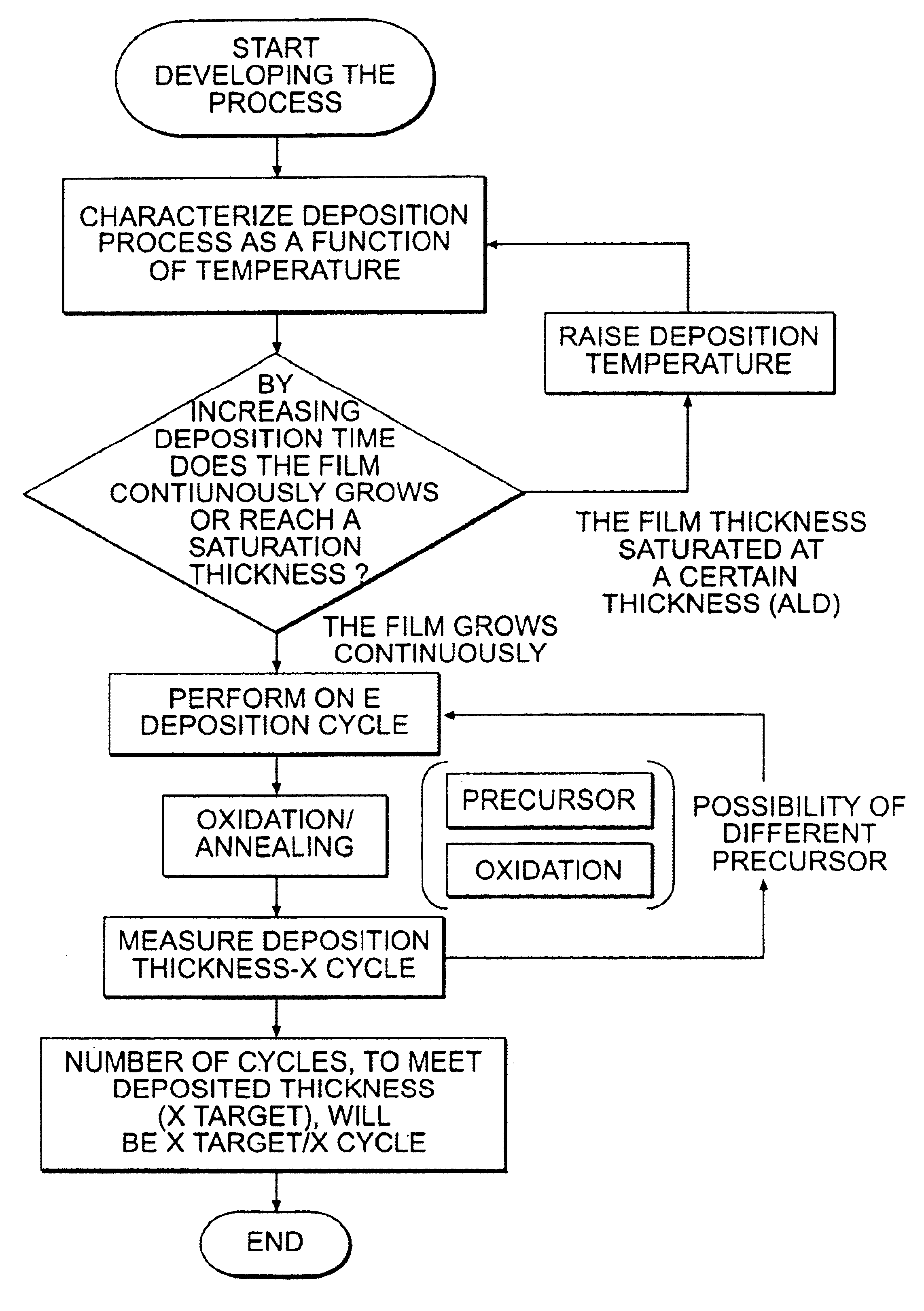
[0037]It is to be understood by one of ordinary skill in the art that the present discussion is a description of exemplary embodiments only, and is not intended as limiting the broader aspects of the present invention, which broader aspects are embodied in the exemplary construction.

[0038]The present invention is generally directed to a method of depositing a coating having a relatively high dielectric constant “k” onto a substrate. For instance, the dielectric constant of the coating formed according to the present invention is typically greater than about 4, in some embodiments greater than about 8, in some embodiments greater than about 10, and in some embodiments, greater than about 15. For instance, coatings formed according to the present invention might have a dielectric constant between about 5 to about 100, and in some embodiments, between about 15 to about 20. Further, the resulting high-k coating can generally have a thickness less than about 30 nanometers. For instance, ...


PUM

PropertyMeasurementUnit
deposition temperatureaaaaaaaaaa
temperatureaaaaaaaaaa

Abstract

A method for depositing a high-k dielectric coating onto a substrate, such as a semiconductor wafer, is provided. The substrate is subjected to one or more reaction cycles. For instance, in a typical reaction cycle, the substrate is heated to a certain deposition temperature. Thereafter, in one embodiment, one or more reactive organo-metallic gas precursors are supplied to the reactor vessel. An oxidizing gas is also supplied to the substrate at a certain oxidizing temperature to oxidize and / or densify the layers. As a result, a metal oxide coating is formed that has a thickness equal to at least about one monolayer, and in some instances, two or more monolayers. The dielectric constant of the resulting metal oxide coating is often greater than about 4, and in some instance, is from about 10 to about 80.

Description

RELATED APPLICATIONS[0001]The present application claims priority to a provisional application filed on Mar. 20, 2001 having Ser. No. 60 / 277,326.BACKGROUND OF THE INVENTION[0002]For forming MOSFET (Metal Oxide Semiconductor Field Effect Transistor) devices or high memory devices, such as DRAMs (Dynamic Random Access Memories), it is often necessary to form a thin, high dielectric constant (high-k) coating onto a substrate, such as a silicon wafer. For example, the thickness of such coatings is often less than 30 nanometers. To form such a thin dielectric coating on a substrate, a variety of deposition techniques have been developed.[0003]For example, chemical vapor deposition (CVD) has traditionally been used to form a high-k coating on a substrate. Chemical vapor deposition typically involves supplying a gas precursor and oxidizing gas to a vessel. The precursors decompose and react with the oxidizing gas on the surface of the substrate to form the oxide coating. However, chemical ...

Claims


Application Information

Patent Timeline
Patent Type & Authority Patents(United States)
IPC IPC(8): B05D3/02C23C16/00H01L21/02H01L21/469H01L21/31C23C16/40C23C16/44C23C16/455C23C16/52H01L21/314H01L21/316
CPCC23C16/40C23C16/45525C23C16/45527C23C16/52H01L21/31604H01L21/3141H01L21/31645H01L21/31637H01L21/31641H01L21/02183H01L21/0228H01L21/02192H01L21/02189H01L21/02159H01L21/02148H01L21/02186H01L21/02181H01L21/02178H01L21/205
Inventor CHANG, JANELIN, YOU-SHENGKEPTEN, AVISHAISENDLER, MICHAELLEVY, SAGYBLOOM, ROBIN
Owner RGT UNIV OF CALIFORNIA
Why Eureka
Try Eureka