Light emitting diode having multiple pits

a light-emitting diode and multiple-pit technology, applied in semiconductor/solid-state device manufacturing, semiconductor devices, electrical apparatus, etc., can solve the problems of increased leakage current, lower overall extraction efficiency, and increased price of superior device stability, so as to improve extraction efficiency, reduce the mean distance to a sidewall, and increase the extraction efficiency of light

Inactive Publication Date: 2005-04-26
SCHOENFELD WINSTON VAUGHAN
View PDF7 Cites 23 Cited by
  • Summary
  • Abstract
  • Description
  • Claims
  • Application Information

AI Technical Summary

Benefits of technology

[0008]One aspect of the invention is that it provides an array of micro-pits, strategically placed across a single LED die, to increase the extraction efficiency of light generated within the die. The micro-pit regions improve extraction efficiency by reducing the mean distance to a sidewall in active regions, and by creating regions of higher transmission at which the semi-transparent contact is not present.
[0010]A preferred embodiment of the invention provides a structure in which optical extraction efficiency is combined with long term operational stability. This structure may comprise a single contiguous passivation layer over the entire top surface of the LED chip. This layer covers the semi-transparent conductive contact, the side of the emitting area, and the bottom of the void regions. Moreover, this layer prevents degradation of the transparent conductive contact. The preferred material for this passivation layer is SiO2. The typical optical index of refraction of this material is 1.45 which is slightly lower than that of commercially used epoxy and silicone encapsulants (n=1.5-1.6), which do not provide effective passivation. The use of a coating having a lower refractive index slightly reduces the extraction angle for light reaching these surfaces, which leads to a lower overall extraction efficiency. This is the price of superior device stability, and directly contradicts the teachings of Thibeault et al.
[0011]An additional feature of preferred embodiments of the invention is that they allow for a significantly increased surface area for heat transfer out of the LED. In an operating LED, heat generation occurs primarily at the p-n junction. This requires that the depth of the pit or void regions in the device is deep enough to allow them to extend through the active region. Additionally, these voids should be produced using a process that does not create significant conductive pathways along the etched surfaces. Such pathways would result in an increased leakage current as the etched surface area increases. This would in turn degrade LED performance and also decrease device reliability.

Problems solved by technology

The use of a coating having a lower refractive index slightly reduces the extraction angle for light reaching these surfaces, which leads to a lower overall extraction efficiency.
This is the price of superior device stability, and directly contradicts the teachings of Thibeault et al.
Such pathways would result in an increased leakage current as the etched surface area increases.
This would in turn degrade LED performance and also decrease device reliability.

Method used


Image

  • Light emitting diode having multiple pits
  • Light emitting diode having multiple pits
  • Light emitting diode having multiple pits

Examples


Embodiment Construction

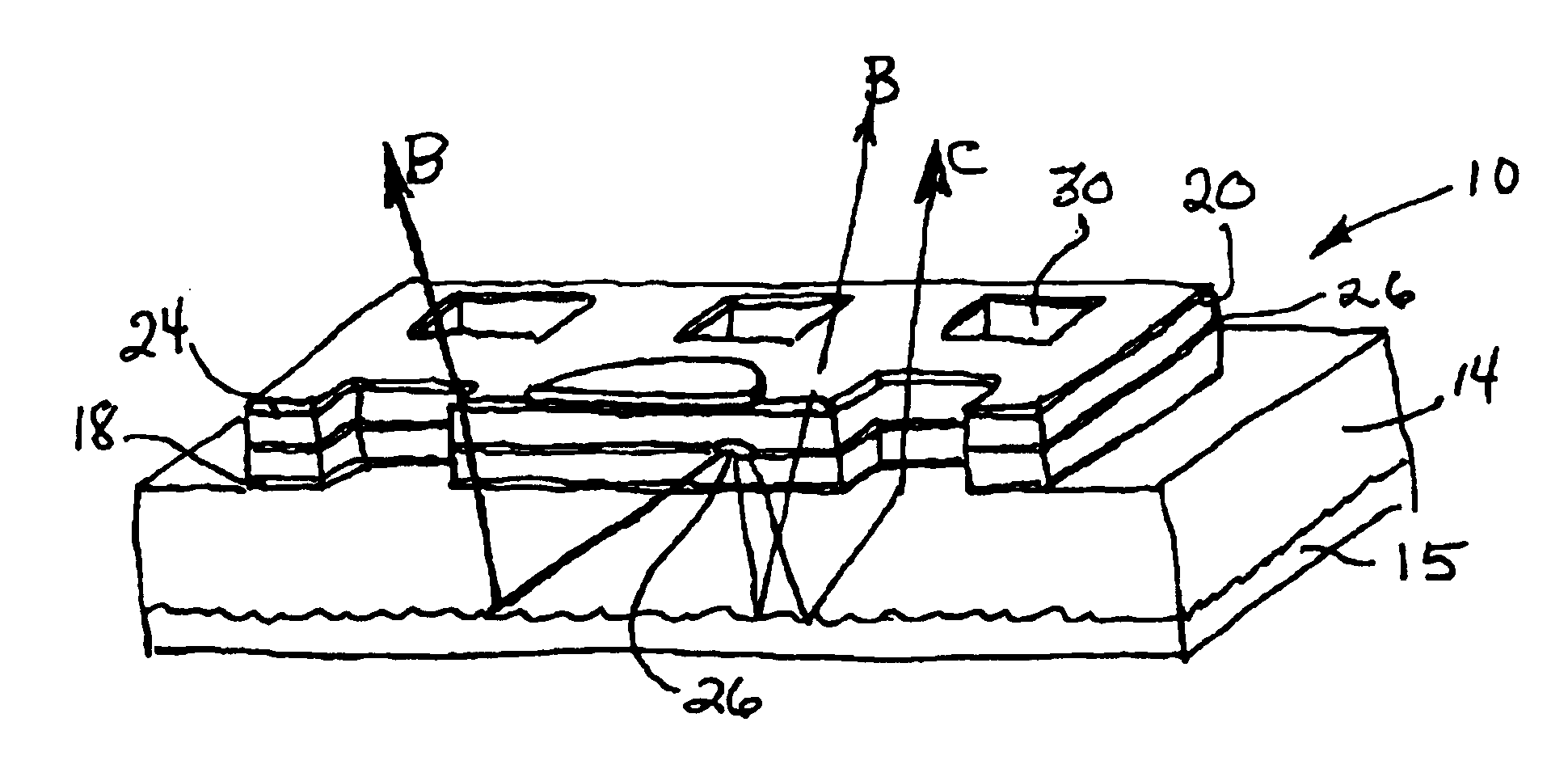
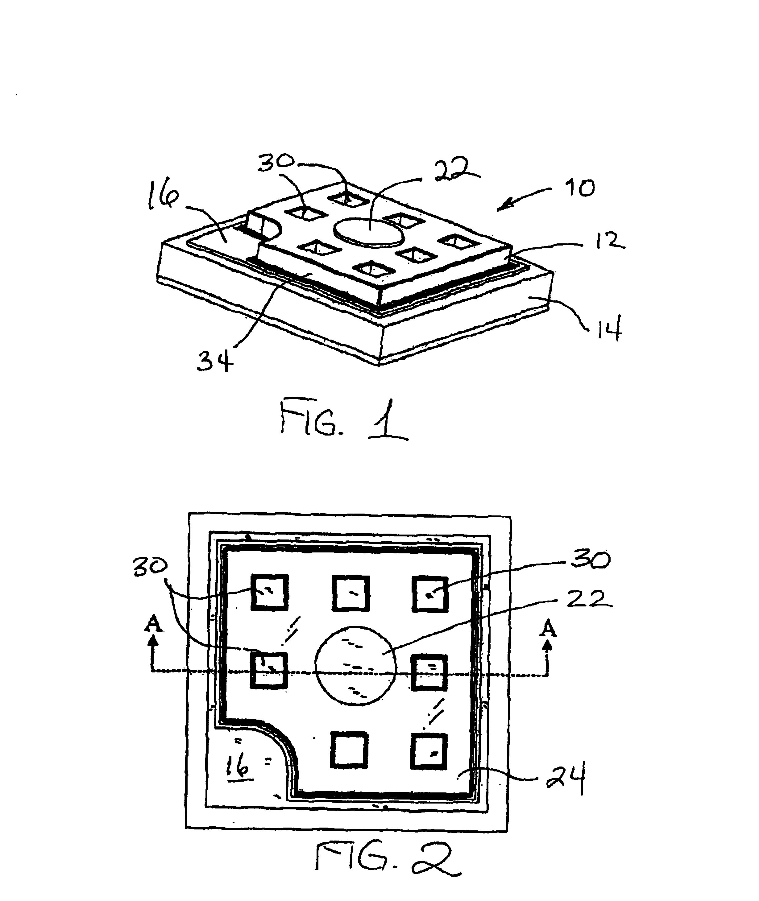
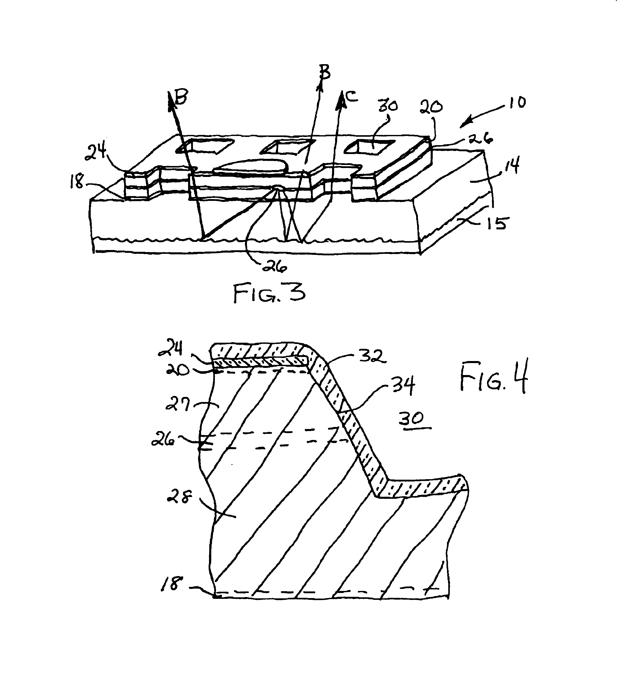
[0018]As is the case with many conventional LEDs, a device of the invention 10 may be formed as a die or mesa 12 extending between two parallel surfaces that, for the purpose of providing the reader with convenient reference to the drawing are referred to as a ‘top’ and ‘bottom’, although the reader will recognize that the LED can be operated in any selected orientation and that the words “top” and “bottom” are used throughout this disclosure to refer to the surface having a semitransparent electrode disposed on it and the surface attached to a substrate, respectively. This die is disposed on a suitable substrate 14 that is preferably transparent and has a reflective bottom surface layer 15 disposed on the surface opposite to the substrate surface to which the die 12 is attached. Electrical contact to the bottom of the mesa 12 is made by lower metallic contact 16 disposed on a heavily doped, low resistivity, semiconductor layer 18. A second electrical contact 20 at the top of the me...


PUM


Abstract

The light extraction efficiency of a Light Emitting Diode (LED) is improved by providing pits etched into a top, emitting, surface of the LED. The presence of the pits reduces the mean distance to a sidewall in active regions, and creates regions of higher transmission at which a semi-transparent contact is not present. The walls of the pits are preferably coated with a passivating layer, such as silicon dioxide, to reduce surface leakage currents and to improve the operational stability of the device at the expense of a reduction in optical extraction efficiency commonly obtained with encapsulants having a higher index of refraction.

Description

BACKGROUND OF THE INVENTION[0001]1. Field of the Invention[0002]This invention relates to light emitting diodes and more particularly to device structures for providing enhanced light extraction efficiency, improved thermal management characteristics, and improved service life.[0003]2. Background Information[0004]Light emitting diodes (LEDs) are a well known class of solid state devices for converting electric energy to light and commonly comprise an active layer of semiconductor material sandwiched between two oppositely doped layers. When a bias is applied across the doped layers, holes and electrons are injected into the active layer where they recombine to generate light, which travels in all directions until it either escapes at an exposed surface, or is reabsorbed.[0005]In U.S. Pat. No. 5,779,924 Krames et al. teach the use of surface texturing on an LED to increase light extraction efficiency through a transparent window layer on a top surface of the LED. This surface texturi...

Claims


Application Information

Patent Timeline
Patent Type & Authority Patents(United States)
IPC IPC(8): H01L29/02H01L29/22H01L33/20H01L33/22
CPCH01L33/20H01L33/22
Inventor SCHOENFELD, WINSTON VAUGHAN
Owner SCHOENFELD WINSTON VAUGHAN
Why Eureka
Try Eureka