Solid-state image sensing device having pixels with barrier layer underneath transistor regions and camera using said device

a solid-state image and sensor technology, applied in the field of solid-state image sensing devices and camera systems, can solve the problems of difficult integration of peripheral circuits such as drive circuits, high power consumption and drive voltage, and high cost, and achieve high spectral sensitivity, less charge leakage, and high reproducibility.

Inactive Publication Date: 2005-04-26
CANON KK
View PDF12 Cites 106 Cited by
  • Summary
  • Abstract
  • Description
  • Claims
  • Application Information

AI Technical Summary

Benefits of technology

[0020]It is an object of the present invention to provide a solid-state image sensing device that has high sensitivity, particularly, for micro pixels, and another object of the present invention is to provide a camera system that are low in power consumption and in drive voltage and low in cost.
[0021]To achieve the foregoing objects, according to a first aspect of the present invention, there is provided a solid-state image sensing device. The solid-state image sensing device has a plurality of pixels. Each pixel includes a photodiode that is constituted by a semiconductor region having a first conductivity type and a semiconductor region having a second conductivity type to generate signal charge. The first conductivity type and the second conductivity type are opposite to each other. Each pixel further includes a first transistor that has a drain region, which has the first conductivity type formed in the second-conductivity-type semiconductor region to transfer the signal charge to the drain region, and a second transistor that has a source region and a drain region, which are formed in the second-conductivity-type semiconductor region and which have the first conductivity type. At least one potential barrier having the second conductivity type is provided under the drain region of the first transistor and the source region and / or the drain region of the second transistor. With arrangement, since the at least one potential barrier is provided under an FD region and the source electrode and / or the drain electrode of each transistor, thereby increasing the sensitivity. This is because signal charge that is generated below the potential barrier is not absorbed by the FD region and the source region and / or the drain region, under which the potential barriers are provided, of each transistor.
[0022]According to a second aspect of the present invention, there is provided a solid-state image sensing device. The solid-state image sensing has at least one pixel. Each pixel includes a photodiode that is constituted by a semiconductor region having a first conductivity type and a semiconductor region having a second conductivity type. The first conductivity type and the second conductivity type are opposite to each other. Each pixel further includes a transistor that has a source region and a drain region which are provided in the first-conductivity-type semiconductor region and which have the first conductivity type. A potential barrier having the second conductivity type is provided under the gate electrode of the transistor. With this arrangement, the potential barrier that is provided under the gate electrode of an n-type transistor, which constitutes the pixel, prevents short-circuiting between the source and drain. The potential barrier also serves to allow the n-type transistor, provided even in an n-type semiconductor region, to operate.

Problems solved by technology

The former, as compared to the latter, are widely used as high-definition image sensing devices, due to their high sensitivity and low noise, but, on the other hand, have some disadvantages.
Specifically, the power consumption and the drive voltage are high and the cost is high since a general semiconductor manufacturing process cannot be used.
Additionally, it is difficult to integrate peripheral circuits, such as a drive circuit.
Additionally, although various improvements have been made to CMOS solid-state image sensing devices, there is still a problem in that the sensitivity is low, particularly, in a device having a small pixel size.
However, since the n-type cathode region is formed in the p well region 12 by ion implantation, the doping concentration cannot be reduced so significantly.
This conventional structure also has a problem in that the n-type cathode 15 cannot be formed with a high doping concentration at a considerably deep position, due to the limitation of depletion behavior of the n-type cathode 15.
Thus, the volume of the n-type cathode, which provides the photodiode, is limited.
Consequently, a sufficient ability of collecting electrons generated from incident light cannot be achieved, resulting in low sensitivity.
Thus, this structure also has a problem in that the sensitivity decreases.
Also, the conventional structure disclosed in U.S. Pat. No. 6,504,193 cannot prevent some of electrons that are generated from incident light from being absorbed by the source and drain of another transistor in the pixel or from being absorbed by adjacent pixels, since the punch-through stopper region is formed only under a signal detection portion.
Thus, this structure also has a problem in that the sensitivity decreases as well.

Method used


Image

  • Solid-state image sensing device having pixels with barrier layer underneath transistor regions and camera using said device
  • Solid-state image sensing device having pixels with barrier layer underneath transistor regions and camera using said device
  • Solid-state image sensing device having pixels with barrier layer underneath transistor regions and camera using said device

Examples


first embodiment

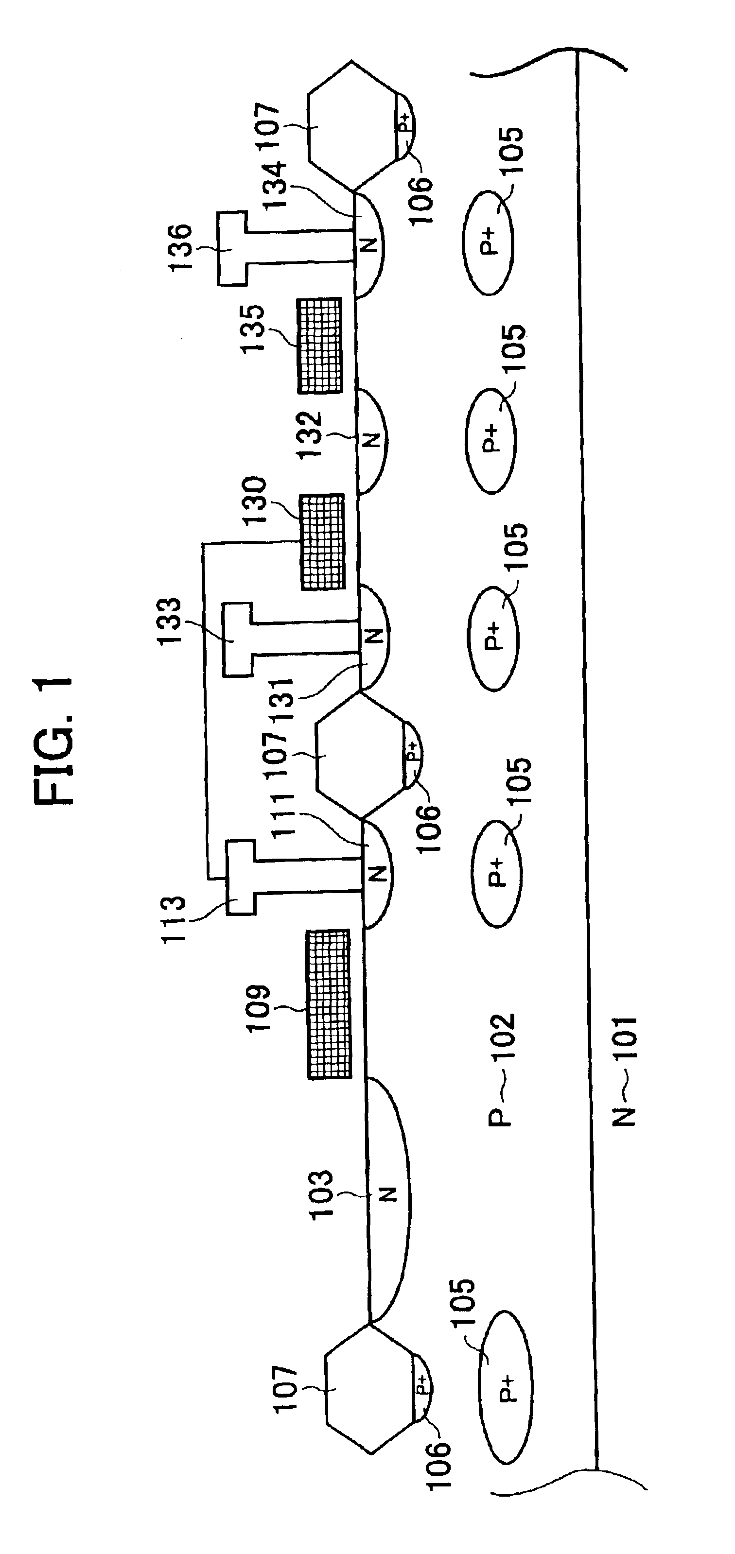
[0053]FIG. 1 is a schematic sectional view of a solid-state image sensing device according to a first embodiment of the present invention.

[0054]In FIG. 1, reference numeral 101 represents a semiconductor substrate having a first-conductivity-type (n-type in this case by way of example), 102 is a p well which is a second-conductivity-type semiconductor region, and 103 is an n-type semiconductor region which is formed in the p well 102 and which is a first-conductivity-type semiconductor region. The p well 102 and the n-type semiconductor region 103 constitute a photodiode. Signal charge that is generated from incident light is stored in the n-type semiconductor region 103. Reference numeral 111 represents a drain region of a transfer transistor, which is a first transistor, for transferring signal charge generated by the photodiode. The drain region has the first conductivity type and serves as an FD region and an n-type semiconductor region formed in the p well 102. Reference numera...

second embodiment

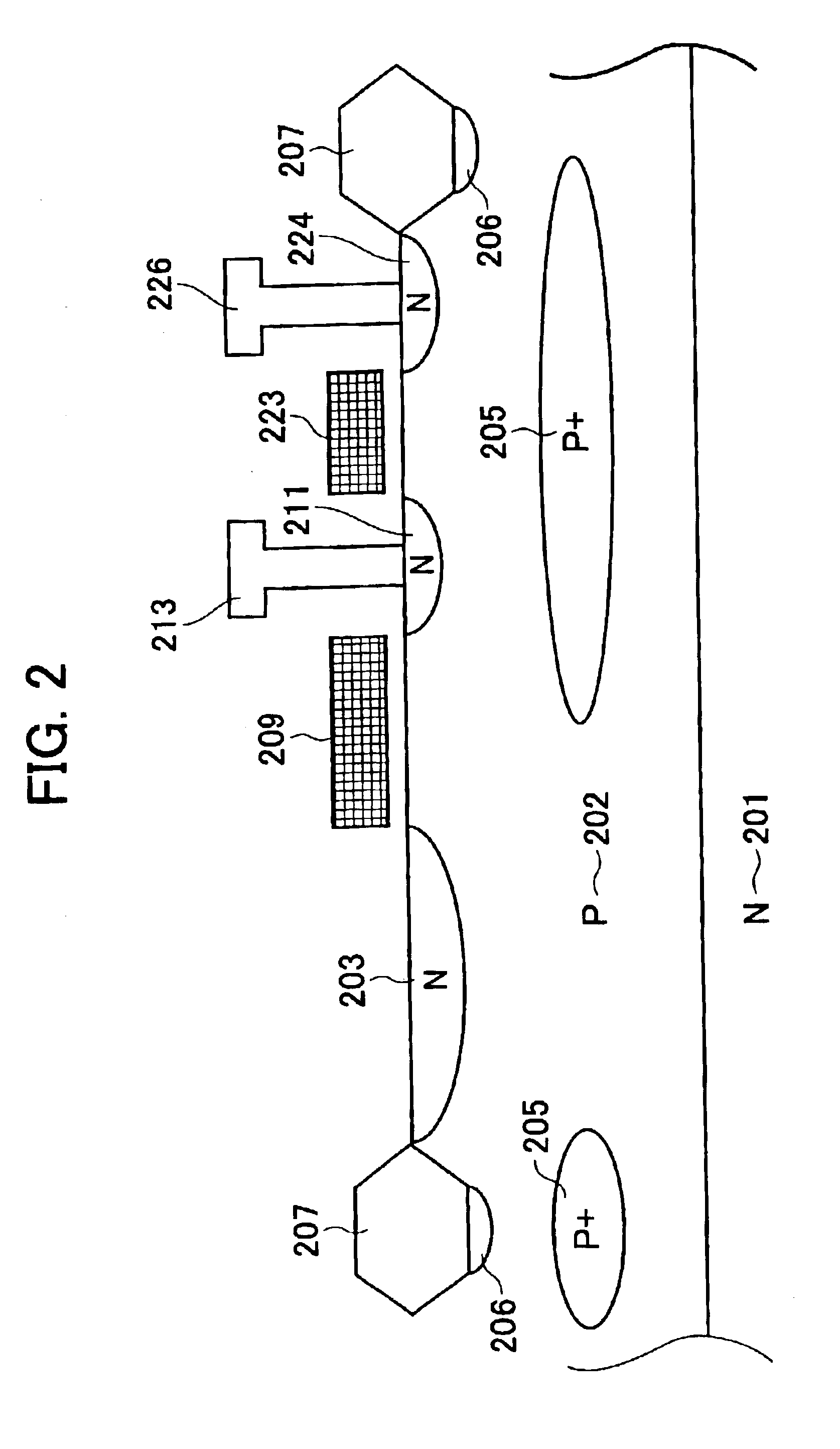
[0064]FIG. 2 is a schematic sectional view of a solid-state image sensing device according to a second embodiment of the present invention.

[0065]More specifically, FIG. 2 is a schematic sectional view of a solid-state image sensing device having a photodiode, a transfer transistor and a reset transistor for resetting an FD electrode 211. Thus, this solid-state image sensing device has a reset transistor, serving as a second transistor, for resetting the FD electrode 211.

[0066]In FIG. 2, reference numeral 223 represents a gate electrode of the reset transistor for resetting the FD electrode 211 and reference numeral 224 represents a drain region of the reset transistor and is connected to a power-supply line 226.

[0067]This embodiment is different from the first embodiment described above in that a potential barrier 205 is also provided under the gate electrode 223 of the second transistor. Thus, the potential barrier 205 reduces the amount of signal charge that is absorbed by n-type ...

third embodiment

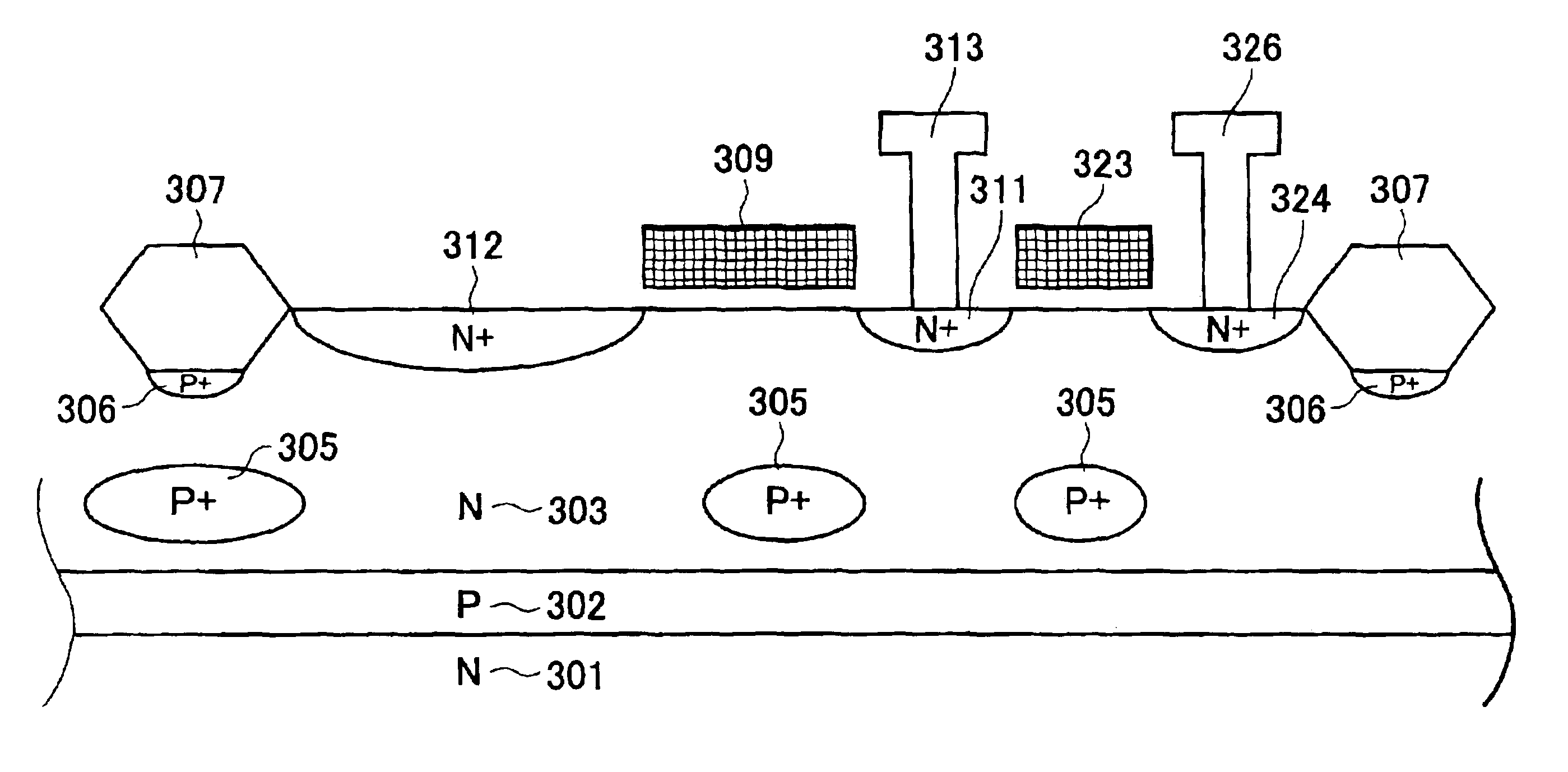
[0075]FIG. 3 is a schematic sectional view of a solid-state image sensing device according to a third embodiment of the present invention.

[0076]Specifically, FIG. 3 is a schematic sectional view of a solid-state image sensing device having a photodiode, a transfer transistor, and a reset transistor for resetting an FD electrode 311.

[0077]Referring to FIG. 3, an n well or n-type semiconductor region 303 is provided as a first-conductivity-type semiconductor region at a layer above an n-type semiconductor substrate 301. A p-type semiconductor region 302 is provided as a second-conductivity-type semiconductor region. The p-type semiconductor region 302 and the n-type semiconductor region 303 constitute a photodiode. A first-conductivity-type signal-charge storing region 312 collects and stores signal charge generated by the photodiode and has a doping concentration higher than the n-type semiconductor region 303.

[0078]The difference between the configurations shown in FIGS. 2 and 3 is ...


PUM


Abstract

A solid-state image sensing device includes a plurality of pixels. Each pixel has a photodiode, a first transistor, and a second transistor. The photodiode is constituted by a first-conductivity-type semiconductor region and a second-conductivity-type semiconductor region. The first and second conductivity types are opposite to each other. The first transistor has a first-conductivity-type drain region formed in the second-conductivity-type semiconductor region to transfer signal charge to the drain region. The second transistor has a source region and a drain region which are formed in the second-conductivity-type semiconductor region and which have the first conductivity type. At least one second-conductivity-type potential barrier is provided under the drain region of the first transistor and the source region and / or the drain region of the second transistor.

Description

BACKGROUND OF THE INVENTION[0001]1. Field of the Invention[0002]The present invention relates to a solid-state image sensing device and a camera system using the same.[0003]2. Description of the Related Art[0004]In recent years, the demand for solid-state image sensing devices has been rapidly increasing for use in image capturing apparatuses, such as, mainly, digital still cameras and video camcorders. As such solid-state image sensing devices, CCDs (Charge Coupled Devices) or MOS solid-state image sensing devices have been used. The former, as compared to the latter, are widely used as high-definition image sensing devices, due to their high sensitivity and low noise, but, on the other hand, have some disadvantages. Specifically, the power consumption and the drive voltage are high and the cost is high since a general semiconductor manufacturing process cannot be used. Additionally, it is difficult to integrate peripheral circuits, such as a drive circuit.[0005]For these reasons, ...

Claims


Application Information

Patent Timeline
Patent Type & Authority Patents(United States)
IPC IPC(8): H01L27/146H04N5/335H04N5/369H04N5/374
CPCH01L27/14609H01L27/1463H01L27/14689H01L27/14643H01L27/14654H01L27/14656H01L27/14632H01L27/14603H01L27/146
Inventor SHINOHARA, MAHITOINOUE, SHUNSUKE
Owner CANON KK
Why Eureka
Try Eureka