Magnetic RAM cell device and array architecture

a technology of array architecture and magnetic ram, which is applied in the field of magnetic ram devices based on magnetic tunnel junction cells, can solve the problems of loss of data or change of switching threshold, significant disadvantage of adding a transistor to each cell, and the requirement for relatively large transistors

Inactive Publication Date: 2005-04-26
TAIWAN SEMICON MFG CO LTD
View PDF8 Cites 26 Cited by
  • Summary
  • Abstract
  • Description
  • Claims
  • Application Information

AI Technical Summary

Benefits of technology

[0014]A principal object of the present invention is to provide an ...

Problems solved by technology

There are two significant problems with this design.
These “half-select” disturbances can cause loss of data or change of switching thresholds.
While this MRAM architecture is a significant improvement over the previous art shown in FIGS. 1-3, the addition of a transistor to each cell is a significant disadvantage.
Further, since both transistors must carry ...

Method used


Image

  • Magnetic RAM cell device and array architecture
  • Magnetic RAM cell device and array architecture
  • Magnetic RAM cell device and array architecture

Examples


first embodiment

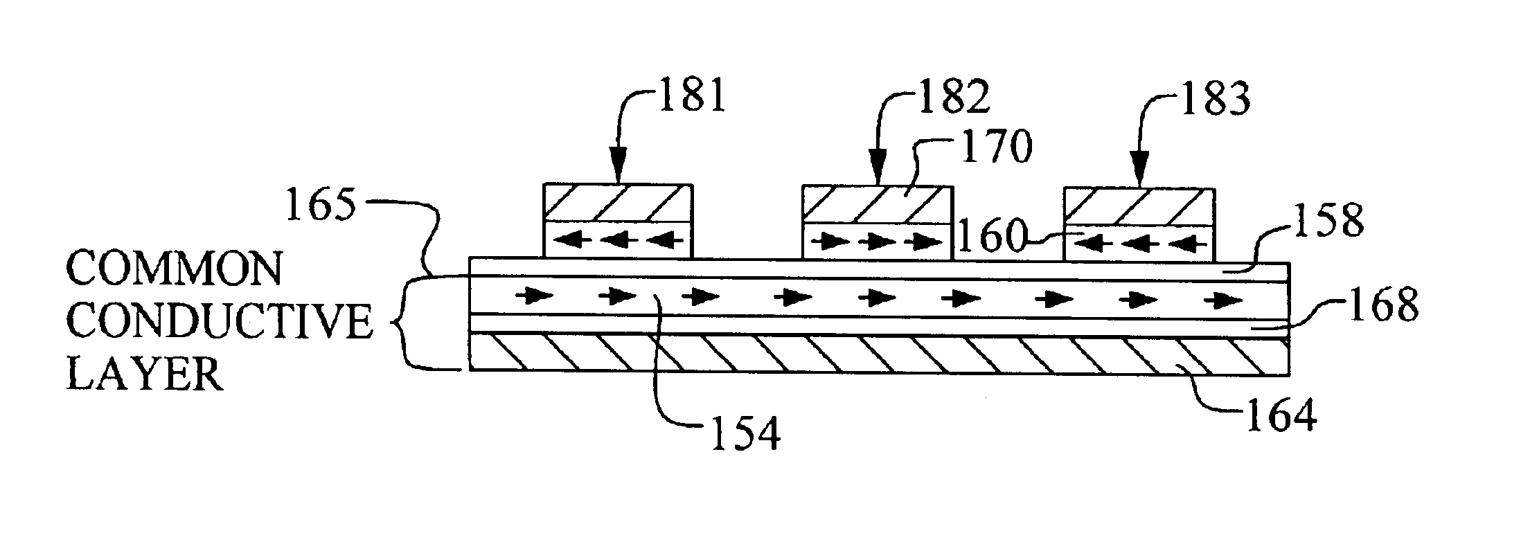
[0041]Referring now to FIG. 5b, a second preferred embodiment of the MTJ cell group is illustrated. In this case, only the free layer 160 and second conductor layer 170 are unique to each cell 181, 182, and 183. The remaining layers, including the dielectric layer 158, and the common conductive layer 165, comprising the pinned layer 154, the anti-ferromagnetic layer 168, and the first conductive layer 164, are conformally formed and not patterned to the individual MTJ cells 181, 182, and 183. In practice, however, it is difficult to stop the free layer 158 etch on the tunnel oxide of the dielectric layer 158 or on the pinned layer 154. Therefore, the method wherein only the common conductive layer 164 extends across the sub-array, as shown in FIG. 5a, is easier to manufacture.

[0042]Referring now to FIG. 6a, a first preferred embodiment of a MRAM array 200 of the present invention is illustrated in a schematic form. The array 200 uses the unique MRAM sub-array comprising, in this exa...

second embodiment

[0047]Referring now to FIG. 6c, and alternative form of the second embodiment MRAM array 240 of the present invention is illustrated in a schematic form. In this case, the gates of the transistors 241, 242, and 243 are connected to a gate select signal G1245 and G2246. This gate select line preferably comprises switches SW3247 and SW4248 so that only the local set of cells R1-R3, is selected. Referring now to FIG. 7, the sub-array 250 is illustrated in a top view. In this view, the common conductive layer 260 underlies each MTJ cell 262 from left to right. The data lines, or bit lines 254, 256, and 258, overlie each cell MTJ cell 262 from top to bottom. To write a cell in the sub-array, a program current IASSIST flows in the common conductive layer 260 from the program line PL to ground GND. Note that the longitudinal axis of each MTJ cell 262 is in the same direction as the direction of the common conductive layer 260. The program current, IASSIST, generates a magnetic field, HASSI...


PUM


Abstract

A new magnetic RAM cell device is achieved. The device comprises a plurality MTJ cells each comprising a free layer and a pinned layer separated by a dielectric layer. A common conductive layer couples together all of the pinned layers of the MJT cell. A first end of the common conductive layer is switchably coupled to a programming line. A second end of the common conductive layer is switchably coupled to a ground. A pluraity of diodes is used. Each diode is coupled between one of the MJT cells and one of a plurality of bit lines.

Description

BACKGROUND OF THE INVENTION[0001](1) Field of the Invention[0002]The invention relates to a magnetic RAM device and, more particularly, to a magnetic RAM device based on a magnetic tunnel junction cell.[0003](2) Description of the Prior Art[0004]Magnetic memory devices, based on magnetic tunnel junction (MTJ) cells, are an important new type of memory technology. Magnetic RAM arrays can be formed on an integrated circuit to provide non-volatility, high speed, low writing energy, infinite write cycles, and immunity to radiation. These advantages make magnetic RAM a technology with great promise.[0005]Referring now to FIG. 1, models of magnetic tunnel junction cells 10 and 30 are illustrated. A magnetic tunnel junction cell 10 and 30 comprises a pinned layer 14, a free layer 18, and a dielectric layer 22. Typically, the free layer 18 and the pinned layer 14 comprise ferromagnetic materials that can be magnetically oriented. The free layer 18 is configured such that the magnetic orient...

Claims


Application Information

Patent Timeline
IPC IPC(8): G11C11/15G11C11/00G11C11/02G11C11/16
CPCG11C11/16
Inventor TANG, DENNY DUAN-LEELIN, WEN-CHIN
Owner TAIWAN SEMICON MFG CO LTD
Why Eureka
Try Eureka