Reduced friction lift pin

a technology of lift pins and friction, applied in the field of lift pins, can solve the problems of affecting the useful life of the pin, affecting and affecting the use so as to reduce the scratching of the lift pin, reduce the wear of components, and improve the design of the lift pin spacing a substrate.

Inactive Publication Date: 2005-05-03
APPLIED MATERIALS INC
View PDF9 Cites 66 Cited by
  • Summary
  • Abstract
  • Description
  • Claims
  • Application Information

AI Technical Summary

Benefits of technology

[0006]An improved lift pin design for spacing a substrate from a substrate support is provided. The lift pin features at least one larger diameter shoulder section that forms a relief region between the pin and a guide hole disposed through a substrate support. The shoulder section minimizes contact between the subs

Problems solved by technology

Integrated circuits have evolved into complex devices that include millions of transistors, capacitors and resistors on a single chip.
One problem that has been observed in the prior art is particle generation attributed to contact between the lift pins and the guide holes as the lift pins move through the substrate support.
Specifically, conta

Method used


Image

  • Reduced friction lift pin
  • Reduced friction lift pin
  • Reduced friction lift pin

Examples


Embodiment Construction

[0011]The present invention generally provides an apparatus for processing a semiconductor substrate. The invention is illustratively utilized in a processing system, such as a TxZ® CVD processing system, available from Applied Materials, Inc., of Santa Clara, Calif. However, it should be understood that the invention may be incorporated into other chamber configurations such as physical vapor deposition chambers, etch chambers, ion implant chambers, and other semiconductor processing chambers.

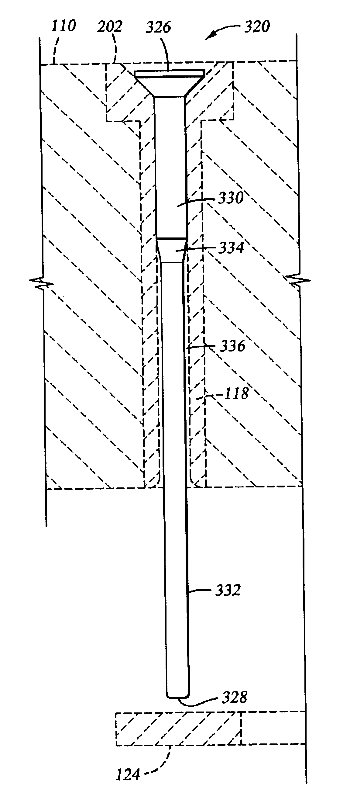
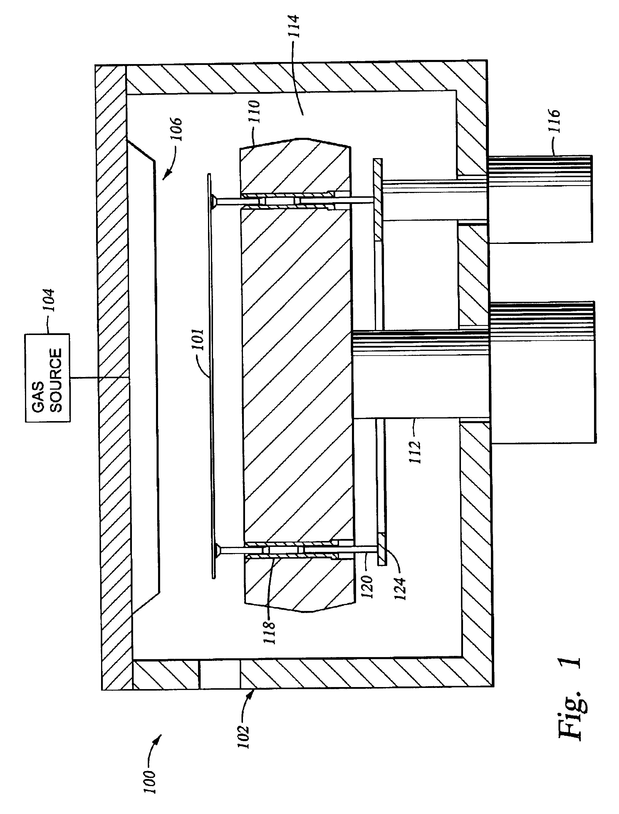
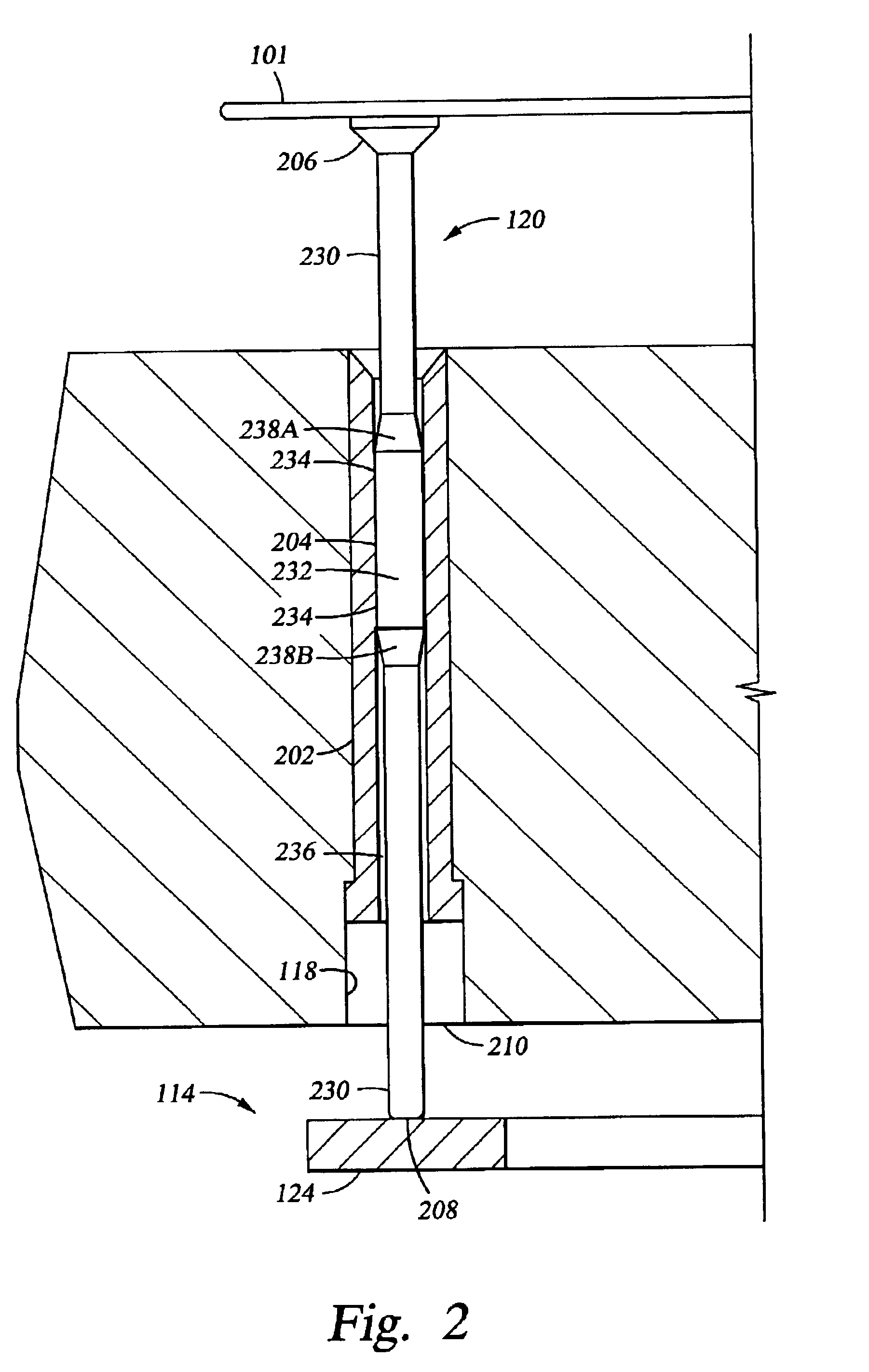
[0012]FIG. 1 depicts a cross sectional view of a processing system 100. The system 100 generally comprises a chamber body 102 coupled to a gas source 104. The chamber body 102 is typically a unitary, machined structure fabricated from a rigid block of material such as aluminum. Within the chamber body 102 is a showerhead 106 and a substrate support assembly 108. The showerhead 106 is coupled to the upper surface or lid of the chamber body 102 and provides a uniform flow of gas from the gas sou...


PUM

PropertyMeasurementUnit
Diameteraaaaaaaaaa
Hardnessaaaaaaaaaa

Abstract

A substrate support is provided that features a lift pin having at least one larger diameter shoulder section that forms a relief region between the lift pin and a guide hole disposed through a substrate support. The shoulder section minimizes contact between the substrate support and lift pin guide hole, thereby reducing pin scratching, particle generation, component wear, and increasing the useful life of the pin. In another embodiment, a flat-bottom tip is provided to promote self-standing of the lift pin, reducing pin tilting or leaning of the lift pin within the guide hole.

Description

FIELD OF THE INVENTION[0001]The present invention relates generally to an apparatus for semiconductor processing. More specifically, the invention relates to a lift pin utilized for spacing substrates from a substrate support.BACKGROUND OF THE INVENTION[0002]Integrated circuits have evolved into complex devices that include millions of transistors, capacitors and resistors on a single chip. The evolution of chip design results in faster circuitry and greater circuit density. As the demand for integrated circuits continues to rise, chip manufactures have demanded semiconductor process tooling having increased wafer throughput, greater product yield, and more robust processing equipment. To meet demands, tooling is being developed to minimize particle contamination and increase the service life of tool components.[0003]One source of particle generation is the lift pins utilized to space a substrate from a substrate support, typically in a processing chamber. The lift pins generally re...

Claims


Application Information

Patent Timeline
IPC IPC(8): C23C16/458C23C16/44H01L21/687H01L21/67
CPCC23C16/4401H01L21/68742C23C16/4583
Inventor OR, DAVID T.KOAI, KEITH K.TAKAHAMA, HIROYUKIITO, TAKAHIROOTA, KOJISATO, HIROSHI
Owner APPLIED MATERIALS INC
Why Eureka
Try Eureka