Method for processing an integrated circuit including placing dice into a carrier and testing

a technology of integrated circuits and dice, applied in the direction of individual semiconductor device testing, semiconductor/solid-state device testing/measurement, instruments, etc., can solve the problems of limited testing of dice, inability to adapt current testing equipment to use with such devices, and high cost and time consumption of packaging processes

Inactive Publication Date: 2005-05-03
FORMFACTOR INC
View PDF65 Cites 107 Cited by
  • Summary
  • Abstract
  • Description
  • Claims
  • Application Information

AI Technical Summary

Problems solved by technology

In a typical manufacturing process, a wafer is subjected to limited testing to identify gross functionality or non-functionality of individual components on the wafer.
The packaging process is both expensive and time consuming.
A key difference is that the die are already packaged once singulated from the wafer, but current testing equipment is not adapted for use with such devices.
Further, a carrier could limit the amount of compression the spring contacts on the die under test underwent, which may be less than the compression allowed during subsequent primary use of the die.

Method used


Image

  • Method for processing an integrated circuit including placing dice into a carrier and testing
  • Method for processing an integrated circuit including placing dice into a carrier and testing
  • Method for processing an integrated circuit including placing dice into a carrier and testing

Examples


Embodiment Construction

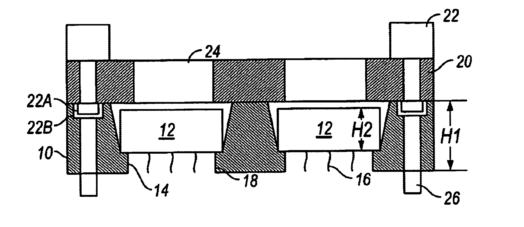
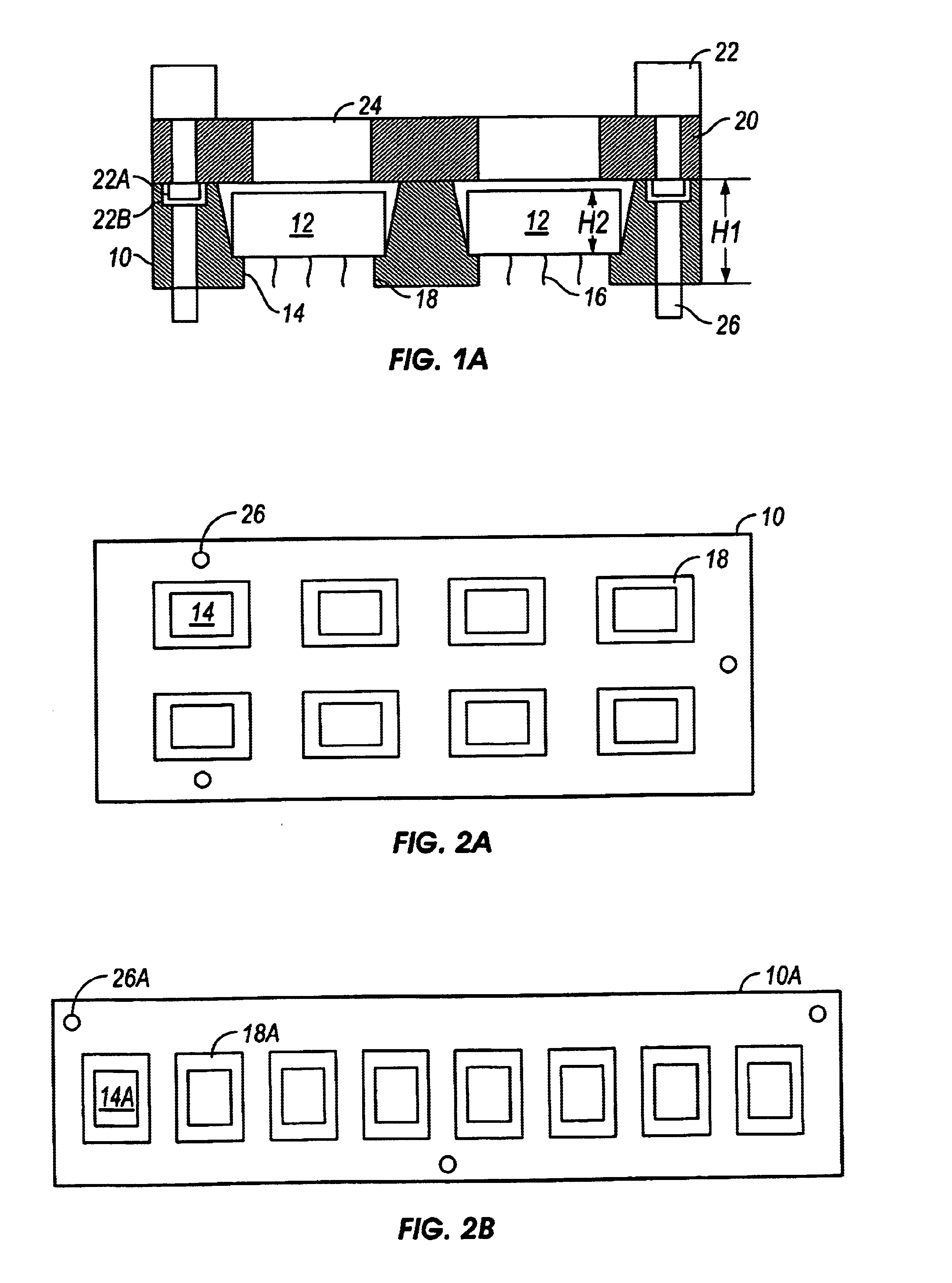
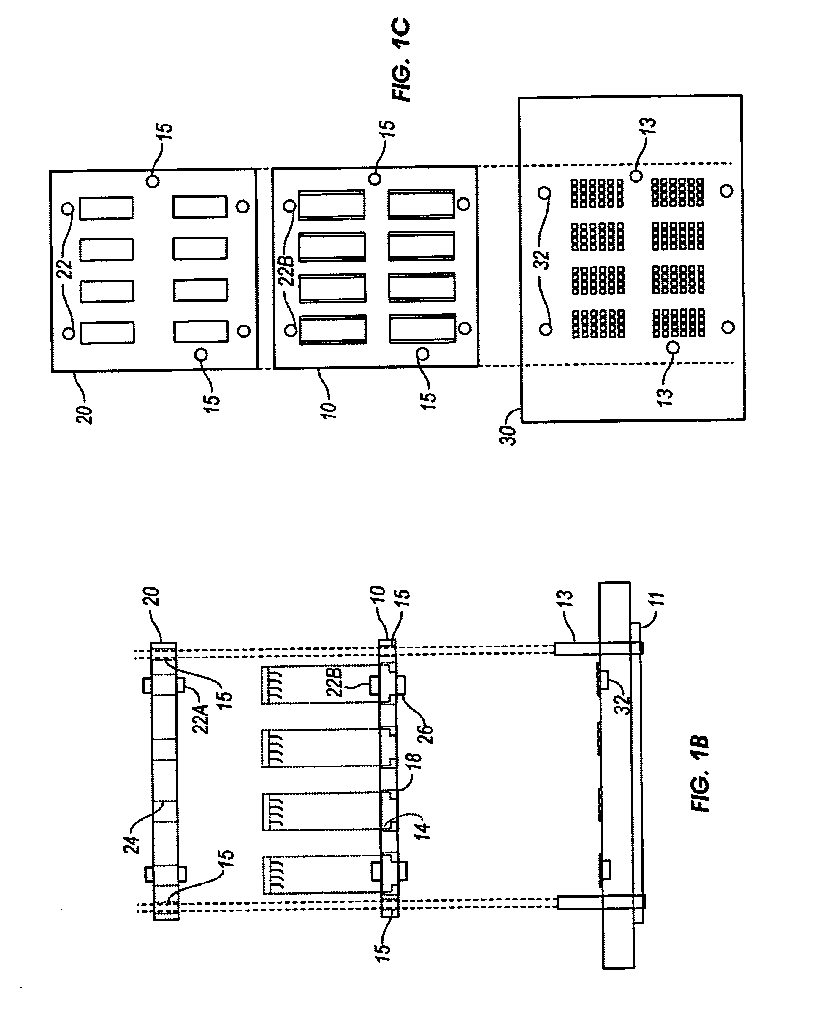
[0045]A method and apparatus for manipulating an integrated circuit (IC) die through testing and a final application is described. A method and apparatus for tracking the die is disclosed. In the following detailed description, numerous specific details are set forth in order to provide a more thorough understanding of the present invention. However, it will be obvious to one skilled in the art that the present invention may be practiced without these specific details. In other instances, well-known devices, methods, procedures, and individual components have not been described in detail so as not to unnecessarily obscure aspects of the present invention.

[0046]The present invention provides a carrier for use in transporting and tracking IC die through testing after they have been cut from the original wafer. The carrier of the present invention is generally used to transport and support the die during testing, and may be labeled to allow for the tracking of both the carrier and its ...


PUM


Abstract

Methods for processing at least one die which comprises an integrated circuit. In one example of a method of the invention, an identification code is applied to a carrier. A singulated die is deposited into the carrier which holds the singulated die. The singulated die comprises an integrated circuit. The identification code may be applied to the carrier before or after depositing the singulated die into the carrier. The carrier may be used in testing the singulated die and may include a plurality of singulated die or just one singulated die. In another example of a method of the invention, an identification code is applied to a die. The die is deposited into a carrier which holds the die. The die comprises an integrated circuit, and the carrier holds the die in singulated form. Typically the die is placed in the carrier without any packaging which may protect the die. The identification code may be applied to the die before or after it is deposited into the carrier.

Description

RELATED APPLICATION[0001]This application is a continuation-in-part of co-pending, commonly assigned U.S. patent application Ser. No. 09 / 205,502, filed Dec. 4, 1998, entitled “Socket for Mating with Electronic Component, Particularly Semiconductor Device with Spring Packaging for Fixturing, Testing, Burning-In.” That application is incorporated herein in full by reference.BACKGROUND OF THE INVENTION[0002]This application is related to the patent application titled “Method for Mounting an Electronic Component” and to the patent application titled “Method for Processing an Integrated Circuit” which are being filed concurrently herewith.[0003]1. Field of the Invention[0004]The present invention relates in general to electronic assemblies and the testing thereof. More specifically, the present invention relates to a method and apparatus for the transport and handling of die from an original wafer to a test board, a printed circuit board, and / or a final product substrate.[0005]2. Descrip...

Claims


Application Information

Patent Timeline
Patent Type & Authority Patents(United States)
IPC IPC(8): G01R1/04G01R1/02H01L23/538H01L23/02H01L23/52H01L23/13H01L23/04H01L23/12H01L23/48H01L23/32H05K3/32G01R31/01G01R31/28B65D85/86G01R31/00G01R31/26H01L21/673H01L23/544
CPCG01R1/0408G01R1/0433G01R1/0466G01R31/2863G01R31/2867H01L21/67294H01L23/04H01L23/13H01L23/32H01L23/5385H01L24/72H05K3/325H01L2924/10253G01R31/01G01R31/2893H01L2223/54473H01L2224/16H01L2924/01013H01L2924/01027H01L2924/01033H01L2924/01079H01L2924/01082H01L2924/14H01L2924/16152H05K2201/09472H01L2924/01006H01L2924/01019H01L2924/01074H01L2924/01075H01L2924/00H01L2924/15787H01L2924/12042H01L2224/73251H01L23/544H01L2924/0002H01L2224/72H05K3/32
Inventor ONDRICEK, DOUGLAS S.PEDERSON, DAVID V.
Owner FORMFACTOR INC
Why Eureka
Try Eureka