Passivation processing over a memory link

a memory link and processing technology, applied in the field of passivation processing over a memory link, can solve the problems of incomplete link severing, deterioration of the quality of the device that includes the severed link, and increased laser pulse energy, so as to improve the processing quality for removal

Inactive Publication Date: 2005-05-03
ELECTRO SCI IND INC
View PDF37 Cites 184 Cited by
  • Summary
  • Abstract
  • Description
  • Claims
  • Application Information

AI Technical Summary

Benefits of technology

[0015]An object of the present invention is to provide a method or apparatus for improving the processing quality for removal of IC links.
[0019]Still another object of the invention is to avoid or minimize substrate damage and undesirable damage to the passivation structure.
[0020]Still another object of the invention is to avoid numerous extra processing steps while removing links with an alternative method to that of explosive laser blowing.
[0021]In International Publication No. WO 01 / 51243, published on Jul. 19, 2001, and U.S. Publication No. 2002-0003130 A1, published Jan. 10, 2002, a burst of ultrashort laser pulses is employed to sever a conductive link in a substantially nonthermal manner that offers a wider processing window, eliminates undesirable HAZ effects, and achieves superior severed link quality. The duration of the burst is preferably in the range of 10 ns to 500 ns; and the pulse width of each laser pulse within the burst is generally shorter than 25 ps, preferably shorter than or equal to 10 ps, and most preferably about 10 ps to 100 fs or shorter. The burst can be treated as a single “pulse” by conventional laser positioning systems to perform on-the-fly link removal without stopping whenever the laser system fires a burst of laser pulses at each selected link.
[0023]The duration of a set having at least one laser pulse is shorter than 1,000 ns, more preferably shorter than 500 ns, and most preferably shorter than 300 ns, and preferably in the range of 5 to 300 ns. Because the whole duration of the set is shorter than 1,000 ns, the set is considered to be a single “pulse” by a traditional link-severing laser positioning system. This practice does not, therefore, entail either a long dwell time or separate duplicative scanning passes of repositioning and refiring at each selected link that would effectively reduce the throughput by factor of about two or more. The laser spot of each of the pulses in the set encompasses the link width and the displacement between the laser spots of each pulse is less than the positioning accuracy of a typical positioning system, which is typically +−0.05 to 0.2 μm. Thus, the laser system can still process the target areas of the passivation layer 44 overlying the target links 22 on-the-fly, i.e. the positioning system does not have to stop moving when the laser system fires a set of laser pulses at a target area of passivation layer 44 over each selected link 22.
[0025]In one embodiment, a continuous wave (CW) mode-locked laser at high laser pulse repetition rate, followed by optical gate and an amplifier, generates sets having one or more ultrashort laser pulses that are preferably from about 100 fs to about 10 ps. In another one embodiment, a Q-switched and CW mode-locked laser generates sets having ultrashort laser pulses that are preferably from about 100 fs to about 10 ps. Because each laser pulse within the set is ultrashort, its interaction with the target materials (passivation layers and metallic link) is substantially not thermal. Each laser pulse breaks off a thin sublayer of about 100-2,000 Å of material, depending on the laser energy or peak power, laser wavelength, and type of material, until the passivation layer 44 over the link 22 is removed. This substantially nonthermal process may mitigate certain irregular and inconsistent link processing quality associated with thermal-stress explosion behavior of passivation layers 44 of links 22 with widths narrower than about 1 μm or links 22 thicker (depthwise) than about 1 μm. In addition to the “nonthermal” and well-controllable nature of ultrashort-pulse laser processing, the most common ultrashort-pulse laser source emits at a wavelength of about 800 nm and facilitates delivery of a small-sized laser spot. Thus, the process may facilitate greater circuit density.

Problems solved by technology

Such a conventional link processing laser pulse creates a large heat affected zone (HAZ) that could deteriorate the quality of the device that includes the severed link.
Increased laser pulse energy increases the damage risk to the IC chip.
However, using a laser pulse energy within the risk-free range on thick links often results in incomplete link severing.

Method used


Image

  • Passivation processing over a memory link
  • Passivation processing over a memory link
  • Passivation processing over a memory link

Examples


Embodiment Construction

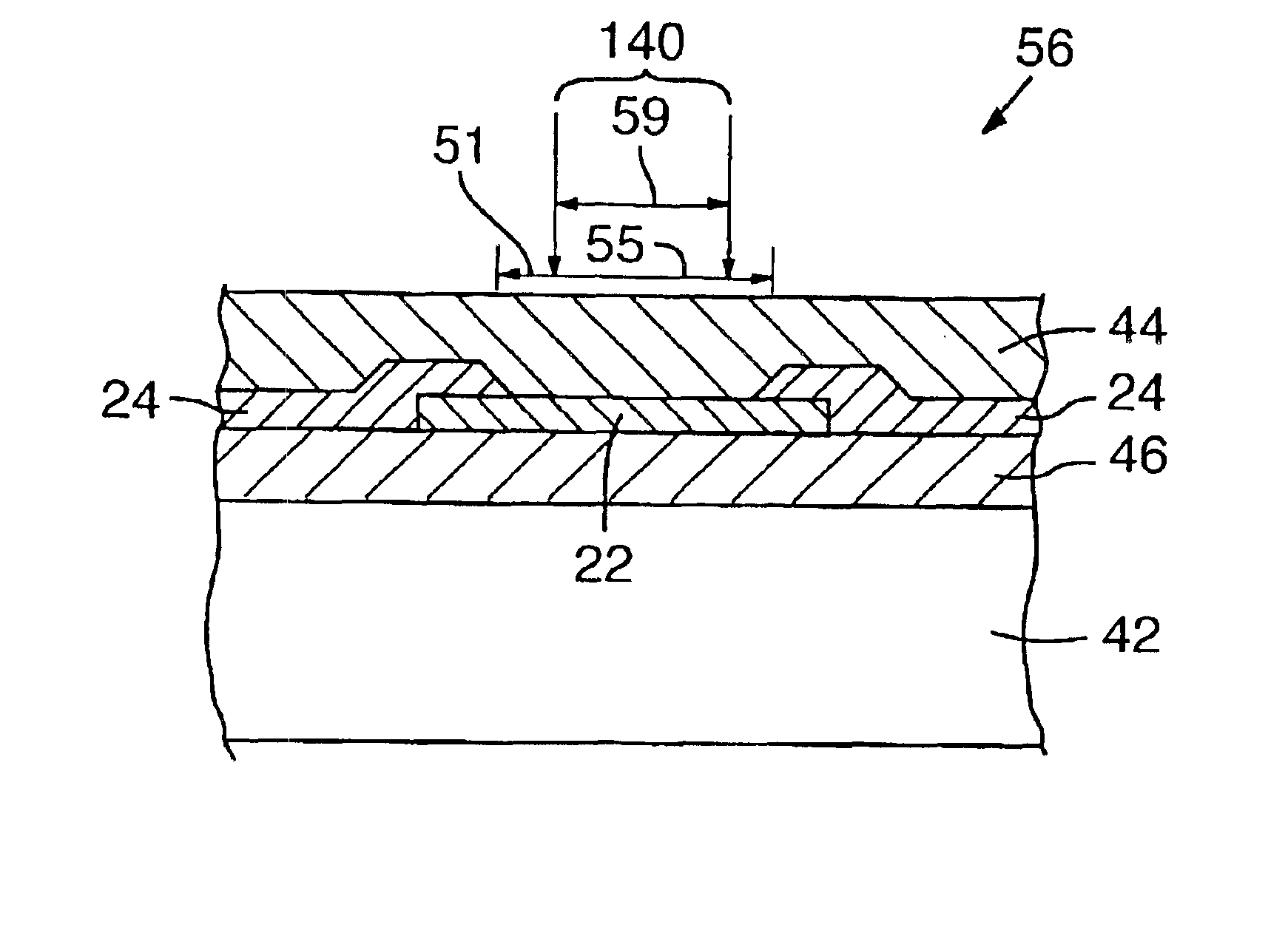
[0043]FIGS. 3A, 3B, and 3C (collectively FIG. 3) are fragmentary cross-sectional side views of target structure 56 undergoing sequential stages of target processing in accordance with the present invention. Target structure 56 can have dimensions as large as or smaller than those blown by laser spots 38 of conventional link-blowing laser output 48. For convenience, certain features of target structure 56 that correspond to features of target structure 36 of FIG. 2A have been designated with the same reference numbers.

[0044]With reference to FIG. 3, target structure 56 comprises an overlying passivation layer 44 that covers an etch target such as link 22 that is formed upon an optional underlying passivation layer 46 above substrate 42. The passivation layer 44 may include any conventionally used passivation materials. Typical passivation materials include silicon dioxide and silicon nitride. The underlying passivation layer 46 may include the same or different passivation material(s...


PUM

PropertyMeasurementUnit
time offsetaaaaaaaaaa
wavelengthaaaaaaaaaa

Abstract

A set (50) of one or more laser pulses (52) is employed to remove passivation layer (44) over a conductive link (22). The link (22) can subsequently be removed by a different process such as chemical etching. The duration of the set (50) is preferably shorter than 1,000 ns; and the pulse width of each laser pulse (52) within the set (50) is preferably within a range of about 0.05 ps to 30 ns. The set (50) can be treated as a single “pulse” by conventional laser positioning systems (62) to perform on-the-fly material removal without stopping whenever the laser system (60) fires a set (50) of laser pulses (52) at each target area (51). Conventional wavelengths in the IR range or their harmonics in the green or UV range can be employed.

Description

RELATED APPLICATIONS[0001]This patent application derives priority from U.S. Provisional Application No. 60 / 355,151, filed Feb. 8, 2002; is a continuation-in-part of U.S. patent application Ser. No. 10 / 322,347, filed Dec. 17, 2002, which claims priority from U.S. Provisional Application No. 60 / 341,744, filed Dec. 17, 2001; and is a continuation-in-part of U.S. patent application Ser. No. 09 / 757,418, filed Jan. 9, 2001 U.S. Pat. No. 6,574,250, which claims priority from both U.S. Provisional Application No. 60 / 223,533, filed Aug. 4, 2000 and U.S. Provisional Application No. 60 / 175,337, filed Jan. 10, 2000.TECHNICAL FIELD[0002]The present invention relates to processing of memory or other IC links and, in particular, to a laser system and method employing a one or more fast laser pulses to remove the passivation over an IC link on-the-fly so that it can be subsequently etched.BACKGROUND OF THE INVENTION[0003]Yields in IC device fabrication processes often incur defects resulting from ...

Claims


Application Information

Patent Timeline
Patent Type & Authority Patents(United States)
IPC IPC(8): B23K26/04H01L23/525H01L23/52B23K26/06
CPCB23K26/04B23K26/0613B23K26/063B23K26/043H01L23/5258H01L2924/09701Y10S438/94H01L2924/0002B23K26/0622H01L2924/00
Inventor SUN, YUNLONGHAINSEY, ROBERT F.SUN, LEI
Owner ELECTRO SCI IND INC
Why Eureka
Try Eureka