Nonvolatile semiconductor memory array with byte-program, byte-erase, and byte-read capabilities

a technology of nonvolatile semiconductors and memory arrays, applied in static storage, digital storage, instruments, etc., can solve the problems of large voltage stress required to program and erase the memory cells of the array, inability to access the memory arrays on a byte basis for programming, erasing and reading the memory arrays, etc., to reduce the high voltage stress, reduce the amount of high voltage, and be more reliable

Inactive Publication Date: 2005-05-03
TAIWAN SEMICON MFG CO LTD
View PDF7 Cites 7 Cited by
  • Summary
  • Abstract
  • Description
  • Claims
  • Application Information

AI Technical Summary

Benefits of technology

[0012]It is further an object of this invention to provide a memory array which is more reliable due to new less stressful ways of voltage biasing the memory cell for programming and erasing.
[0013]It is further an object of this invention to provide a memory array which is partitioned into sub-arrays with separate supply voltages so as to lessen the amount of high voltage which is applied to the semiconductor chip at any given time.
[0014]The objects of this invention are achieved by a memory array and its peripheral circuit with byte access capability and containing a local word line driver 0, which connects to control gates of memory cells which store data on bit lines 0-7, a local word line driver 1, which connects to the control gates of memory cells which store data on bit lines 8-15, a local source line driver 0, which connects to source lines of memory cells which store data on bit lines 0-7, a local source line driver 1, which connects to source lines of memory cells which store data on bit lines 8-15, a floating gate memory cell whose drain is connected to a bit line and whose source is connected to said local source line driver, and whose control gate is connected to said local word line driver, bit lines for a first byte of memory which are the drains of said floating gate memory cell, and bit lines for a second byte of memory which are the drains of said floating gate memory cell. The memory array and its peripheral circuit with byte-erase capability also contains a global word line primary input, which feeds two gates of two metal oxide semiconductor field effect transistor MOSFET devices located in said local word line driver circuit, a global source line primary input which feeds two gates of two MOSFET devices located in said local source line driver circuits, a voltage source for said local source line driver circuit, a voltage source for said local word line driver circuit, and a variable, virtual ground for said local word line driver circuit. The memory array and its peripheral circuit also contain bit line outputs, local word lines, and local source lines.
[0015]The memory array and its peripheral circuit with byte-erase capability has one word line switch for each byte of memory. The memory array and its peripheral circuit with byte-erase capability has one source line switch for each byte of memory. The memory array and its peripheral circuit have its even and odd rows physically separated in the semiconductor material to prevent punch-through problems. The memory array has a variable and virtual ground power supply which is used to reduce the high voltage stress on the High Voltage memory cell device. In addition, the memory array is partitioned into sub-arrays. The memory array is divided into sub-arrays which are composed of eight columns of memory cells. There are local word line driver circuits which share a dedicated power supply. Also, there are local source line driver circuits share a dedicated power supply which is different than said dedicated word line driver circuit dedicated power supply. High voltage is only applied to the power of a selected sub-array. This lessens the cumulative voltage stressing on the semiconductor chip and enhances overall chip reliability.

Problems solved by technology

The main deficiencies of the prior art are the inability to access the memory arrays on a byte basis for programming, erasing and reading the memory arrays.
Another deficiency of the prior art is the large amount of voltage stress required to program and erase the memory cells of the array.

Method used


Image

  • Nonvolatile semiconductor memory array with byte-program, byte-erase, and byte-read capabilities
  • Nonvolatile semiconductor memory array with byte-program, byte-erase, and byte-read capabilities
  • Nonvolatile semiconductor memory array with byte-program, byte-erase, and byte-read capabilities

Examples


Embodiment Construction

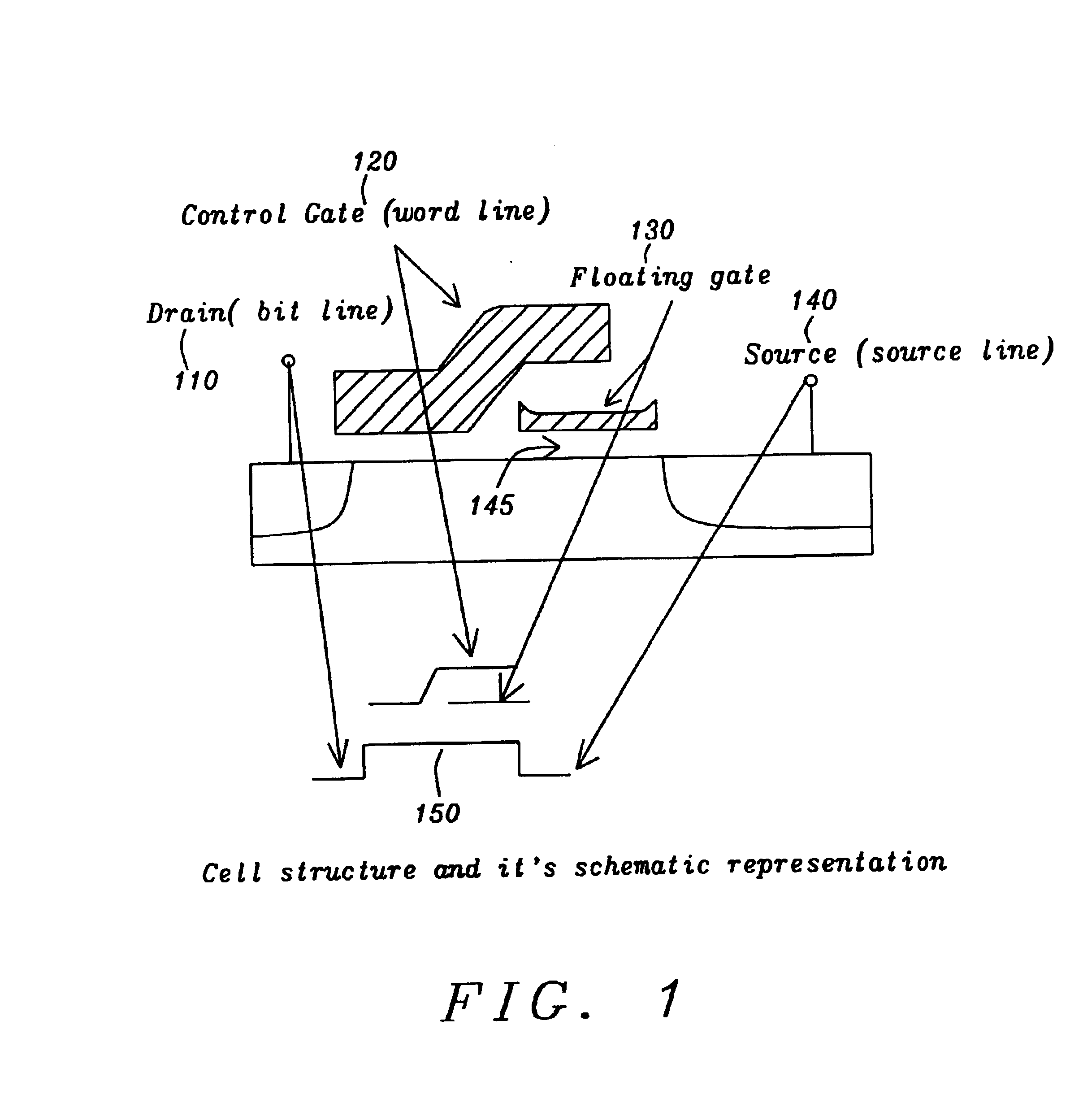
[0021]FIG. 1 shows a cross-sectional view of the floating gate memory cell of this invention. Below this cross-sectional view is the device symbol representation. The floating gate 130 is shown in two views. The upper view shows the floating gate made of poly-silicon over an oxide region 145. The lower view shows the device symbol of the floating gate 130. The drain 110 of the FET memory cell is shown, attached to a bit line. Also, the source 140 is shown attached to a source line, which comes from a source line driver circuit. The control gate 120 is shown in FIG. 1. It is attached to a word line which comes from a word line driver circuit.

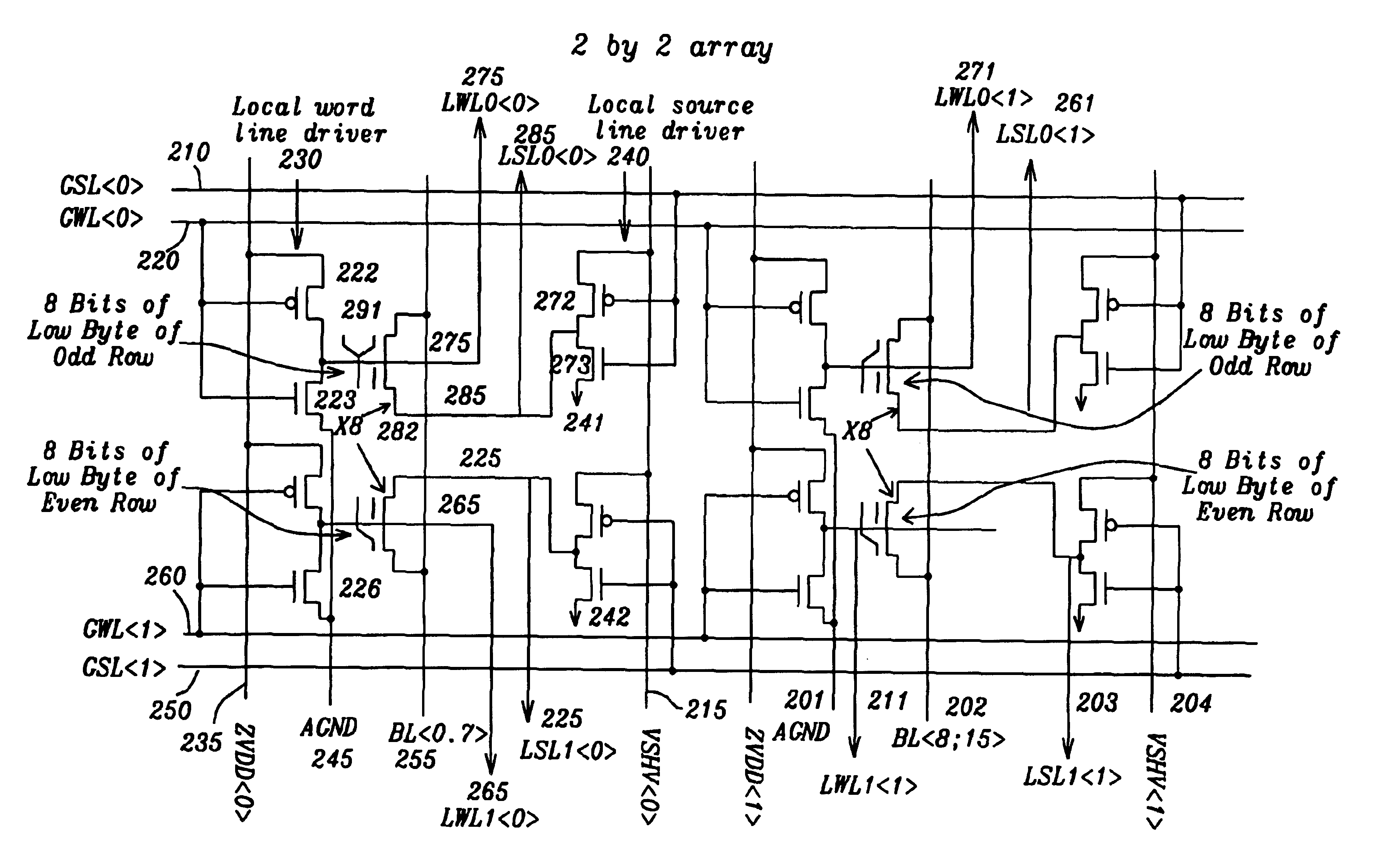
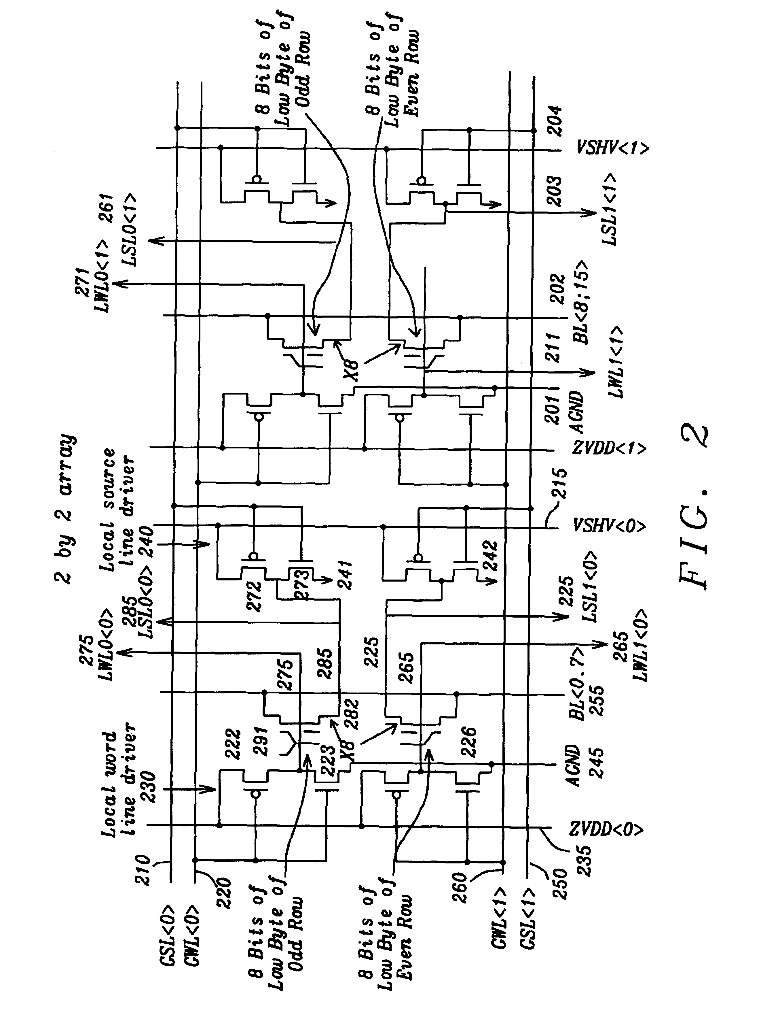
[0022]FIG. 2 shows a 2 by 2 memory array of this invention. The primary inputs include global word lines GWL0>, GWL1>220, 260, which drive the gates of FET devices in the local word line driver circuits 230. The global source lines such as GSL0>210 is a primary input which drives the gates of FET devices in local source line driver circuits. The ...


PUM


Abstract

This invention provides a memory array and its peripheral circuit with byte-erase capability. The advantage of this invention is the ability to access bytes for program, erase, and read operations. This invention allows this access with the addition of one word line switch and one source line switch for each byte to be accessed for program, erase, and read operations. Also, this invention utilizes a new bias condition to lessen the voltage stress on the high voltage device. In addition, this invention utilizes separate and dedicated power supplies for the local word line driver circuits and for the local source line driver circuits. This is coupled with the partitioning of the main memory array into sub-arrays of 8 columns. This allows the placing of high voltage only on the selected 8 column (byte) subarray. This also substantially lessens the voltage stress on the memory cells and enhances long-term reliability.

Description

BACKGROUND OF THE INVENTION[0001]1. Field of the Invention[0002]This invention relates to a memory array and peripheral circuits and methods for writeable memory technologies.[0003]More particularly this invention relates to providing a memory array and peripheral circuits which allow byte access for programming, erasing and reading.[0004]In addition, this invention relates to the ability of providing enhanced long-term reliability for memory arrays by reducing the cumulative voltage stressing of writeable memory arrays.[0005]2. Description of Related Art[0006]Memory cells which can be programmed and erased and re-programmed are known as Electrically, Erasable Programmable Read Only Memory, EEPROM. In the prior art, there are known types of memory arrays and peripheral circuits which are used with EEPROM, flash memory, or non-volatile memory. The main deficiencies of the prior art are the inability to access the memory arrays on a byte basis for programming, erasing and reading the ...

Claims


Application Information

Patent Timeline
Patent Type & Authority Patents(United States)
IPC IPC(8): G11C16/16G11C8/00G11C16/06
CPCG11C16/16G11C16/0425
Inventor CHIH, YUE-DERCHANG, SHU-CHENCHEN, HSIAO-HUI
Owner TAIWAN SEMICON MFG CO LTD
Why Eureka
Try Eureka