Semiconductor memory device and its testing method

a memory device and memory technology, applied in the direction of electronic circuit testing, digital storage, instruments, etc., can solve the problems of limiting the cost reduction, and hardly allowing a more small decrease in the cost per bit of memory

Inactive Publication Date: 2005-05-03
RENESAS ELECTRONICS CORP
View PDF2 Cites 26 Cited by
  • Summary
  • Abstract
  • Description
  • Claims
  • Application Information

AI Technical Summary

Benefits of technology

[0019]It is an object to provide a semiconductor memory device which can eliminate any fault result of a multi-bit test resulting from the coupling noises produced between two adjacent lines of a data bus and a method of testing the semiconductor memory device.
[0021]Accordingly, the “L(Hi-Z)” level on the lines which may undesirably be elevated by the effect of coupling noises resulting from the parasitic capacitance C induced between any two adjacent lines of the data bus, can be maintained to a low level enough not to recognized as the “H” level. As a result, any fault judgment of the multi-bit test caused by the effect of coupling noises generated between the lines of the data bus can successfully be eliminated.

Problems solved by technology

It is however known that as advanced memories for mass storage are developed, their testing process now claims a considerable length of time.
This may inhibit the cost reduction, hence hardly permitting more decrease in the cost per bit of memories.
As a result, its level is detected as “H” level and may interrupt the pass / fail operation of the DQ input / output circuit 84 thus leading to a fault decision.

Method used


Image

  • Semiconductor memory device and its testing method
  • Semiconductor memory device and its testing method
  • Semiconductor memory device and its testing method

Examples


first embodiment

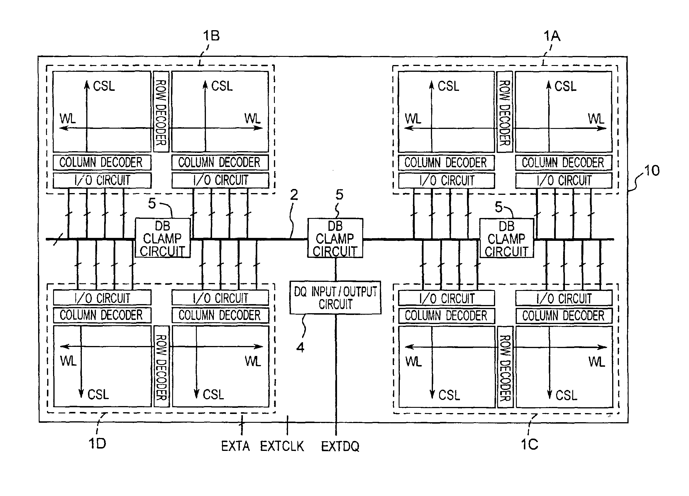
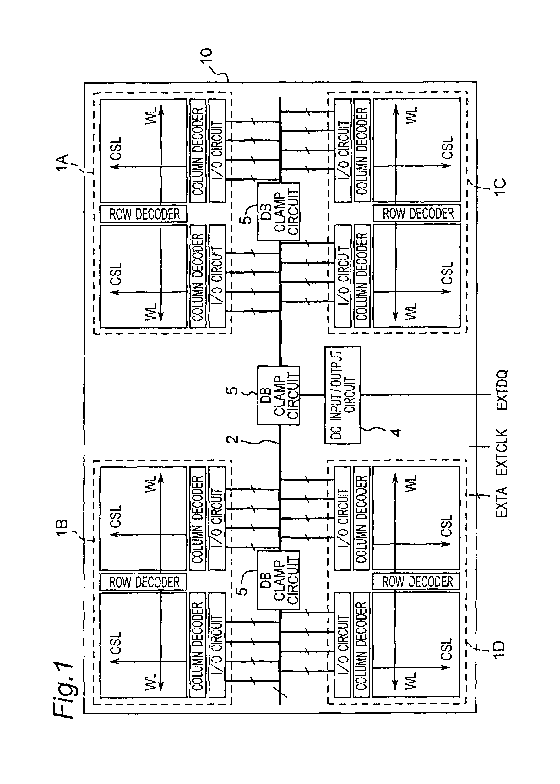
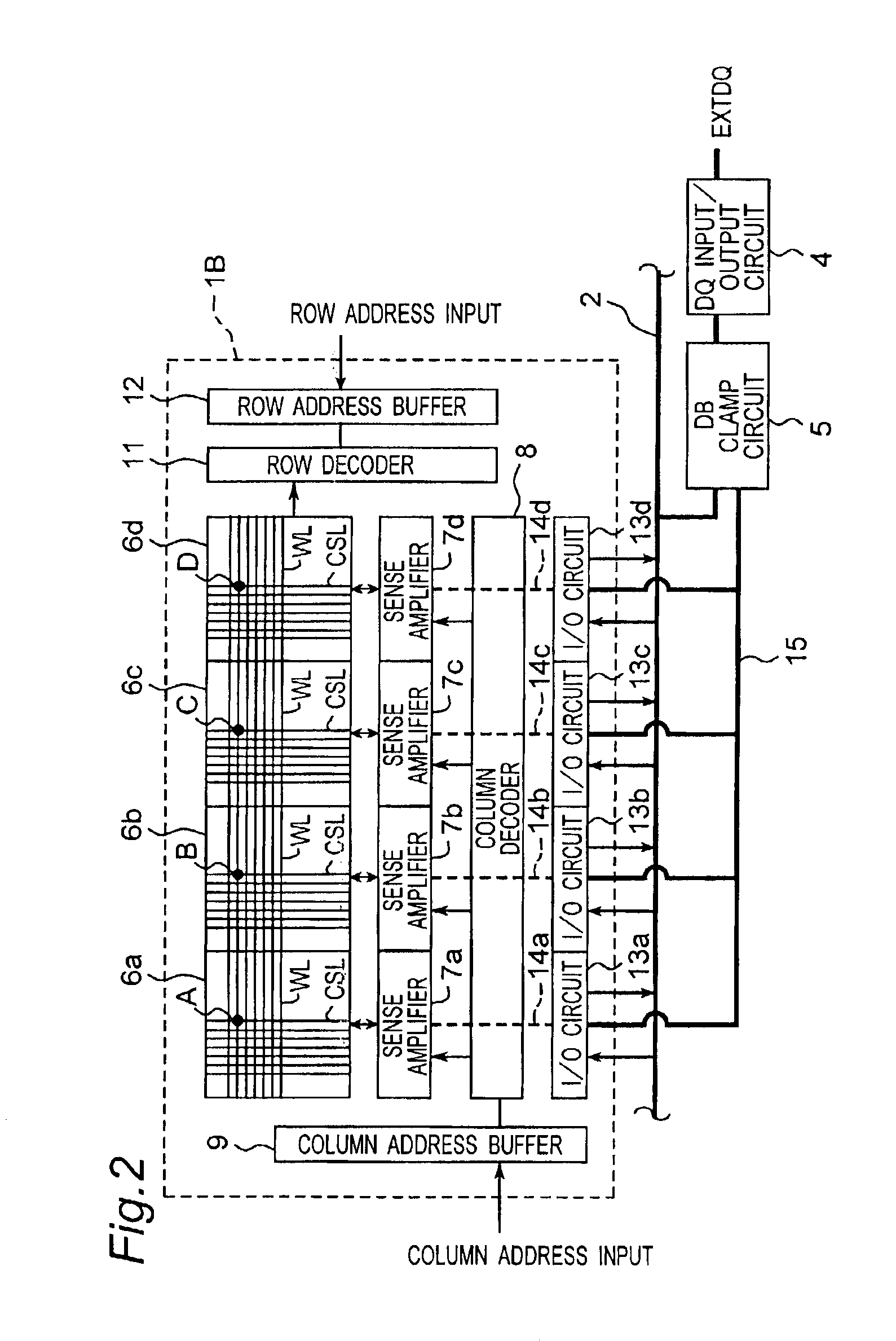
[0043]FIG. 1 illustrates an overall arrangement of a semiconductor memory device according to first embodiment of the present invention. The semiconductor memory device denoted by 10 has four memory array banks 1A to 1D provided in the form of a memory chip which are switched from one to another for storage operation. Each of the memory array banks 1A to 1D includes a plurality of memory arrays (only two shown in FIG. 1). Each memory array is connected by a data bus 2 to a DQ input / output circuit 4 for transmitting data between the memory array and the outside.

[0044]Also, DB clamp circuits 5 are provided across the data bus 2 between the memory array banks 1A to ID and the DQ circuit 4 for attenuating the effect of coupling noises caused by the parasitic capacitance in their adjacent lines of the data bus 2, as will be explained later in more detail.

[0045]In an operation of the semiconductor memory device 10, information data EXTDQ received from the outside are transmitted via an in...

second embodiment

[0050]As described above, by providing the N-channel transistors between any two relevant lines of the data bus 2, the level of lines on “L(Hi-Z)” side can be reduced. At the time, on “H” side, a through current can flow from the drain to the ground GND via the lines of the data bus 2. Accordingly, the multi-bit test may be interrupted by the through current, depending on the gate length (L) and width (W) of the N-channel transistors. For eliminating this drawback, in second embodiment, the DB clamp circuits having a modified arrangement as follows is provided.

[0051]FIG. 5 illustrates the modified DB clamp circuit according to second embodiment. The modified DB clamp circuit 20 has two or more N-channel transistors provided in parallel between adjacent lines of the data bus 2 (only two shown in FIG. 5). Also, a switch (denoted by “AL SW”) is provided between the drain of each N-channel transistor and the line DB or ZDB.

[0052]The DB clamp circuit 20 allows the operation mode of the N...

third embodiment

[0055]FIG. 8 illustrates a delay circuit provided in each of the I / O circuits 13a to 13d for making the activation period of the DB clamp circuit variable, according to third embodiment of the present invention. The delay circuit denoted by 50 delays by a few nanoseconds the output of a pulse signal to the drive bus 15 shown in FIG. 2 from the start of energizing the line DB of the data bus 2, that is, from the leading edge of a PDD (i.e. data bus drive signal) in the DB drive circuit (See FIG. 12) incorporated in each of the I / O circuits 13a to 13d.

[0056]As a result, the input of the pulse signal to the gate of the N-channel transistor in the DB clamp circuit is delayed, i.e. the timing of turning the N-channel transistor on is delayed by a few nanoseconds from the start of energizing the line DB of the data bus 2. This causes the time required for increasing the line DB driven on “H” side to a CMOS level to be shorter than that of first embodiment (where the N-channel transistor ...


PUM


Abstract

A semiconductor memory device is of a bank switching type having a plurality of memory array banks provided in a memory chip which can be switched from one to another for storage operation. The semiconductor memory device includes: a plurality of memory arrays in the memory array banks; an input / output circuit for transmitting information data between the memory arrays and the outside; a data bus for connecting between the memory arrays and the input / output circuit; and N-channel transistors provided across the data bus. The data bus consists of a plurality of adjacent lines. Each of N-channel transistors is connected at their drain to the corresponding lines of the data bus while at their source to the ground. When a multi-bit test is commenced for writing and reading data on the memory arrays, the N-channel transistors are turned on to connect the lines of the data bus to the ground.

Description

BACKGROUND OF THE INVENTION[0001]1. Field of the Invention[0002]The present invention relates to a semiconductor memory device having a plurality of memory cell arrays, e.g., in the form of DRAMs in a memory chip, and a method of testing the semiconductor memory device.[0003]2. Description of the Related Art[0004]In recent years, as highly integral circuit technologies have been introduced in the semiconductor industries, the cost per bit of memories is significantly decreased. However, the increasing demand for memory device now requires an advanced technology for more reduction of the cost. It is however known that as advanced memories for mass storage are developed, their testing process now claims a considerable length of time. This may inhibit the cost reduction, hence hardly permitting more decrease in the cost per bit of memories.[0005]For overcoming the foregoing drawback, some methods are proposed of reducing the time required for testing a semiconductor memory device of ba...

Claims


Application Information

Patent Timeline
Patent Type & Authority Patents(United States)
IPC IPC(8): G11C29/04G11C29/28G01R31/28G11C11/401G11C11/409G11C29/00G11C29/34
CPCG11C29/28G11C2029/2602G11C29/00
Inventor SUZUKI, TAKANOBUTSURUDA, TAMAKIHAYASHI, KATSUSHIGE
Owner RENESAS ELECTRONICS CORP
Why Eureka
Try Eureka