Method for forming an electrostatically-doped carbon nanotube device

a carbon nanotube and electrostatic technology, applied in nanoinformatics, solid-state devices, instruments, etc., can solve problems such as reducing the performance characteristics of nano-scale electronic devices, and achieve the effect of improving the performance characteristics

Inactive Publication Date: 2005-05-10
GENERAL ELECTRIC CO
View PDF2 Cites 130 Cited by
  • Summary
  • Abstract
  • Description
  • Claims
  • Application Information

AI Technical Summary

Benefits of technology

[0005]The present invention provides a method and associated structure for forming an electrostatically-doped carbon nanotube device having well characterized p-type regions and n-type regions, allowing for the creation of nanoscale electronic devices, such as light-emitting diodes (“LEDs”) and the like, with enhanced performance characteristics. More specifically, the present invention provides for the use of a plurality of doping electrodes that are decoupled from a plurality of bias electrodes. Thus, the doping of a carbon nanotube may be finely tuned by varying the bias of each of the plurality of bias electrodes. Advantageously, the method and associated structure of the present invention are capable of providing a carbon nanotube having a P-N junction, a P-I-P junction, a P-I-N junction, an N-I-P junction, an N-I-N junction, a P-N-P junction or an N-P-N junction.

Problems solved by technology

The chemical methods for doping a carbon nanotube, however, suffer from the problem that the p-type regions and the n-type regions are typically not well characterized, resulting in nanoscale electronic devices with reduced performance characteristics.

Method used


Image

  • Method for forming an electrostatically-doped carbon nanotube device
  • Method for forming an electrostatically-doped carbon nanotube device
  • Method for forming an electrostatically-doped carbon nanotube device

Examples


Embodiment Construction

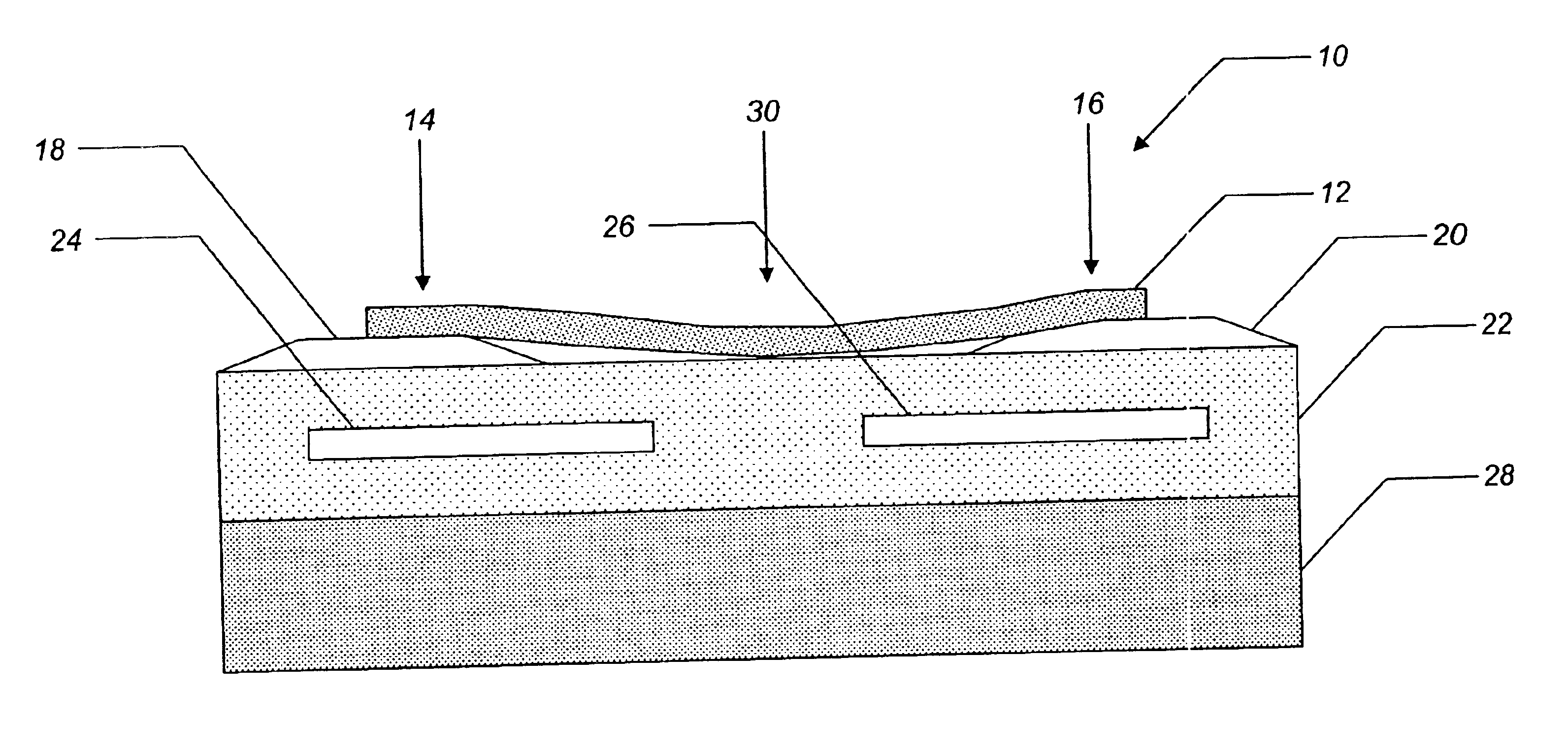
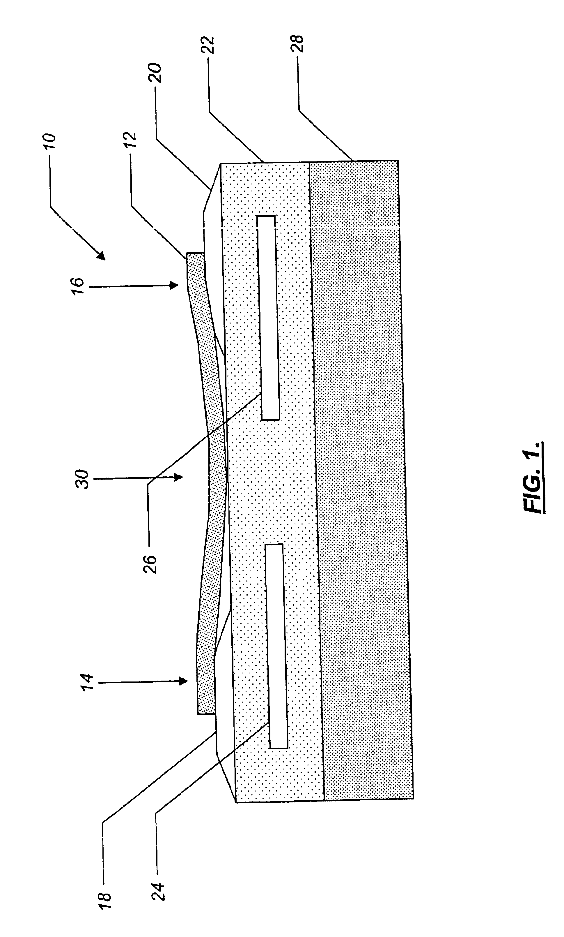
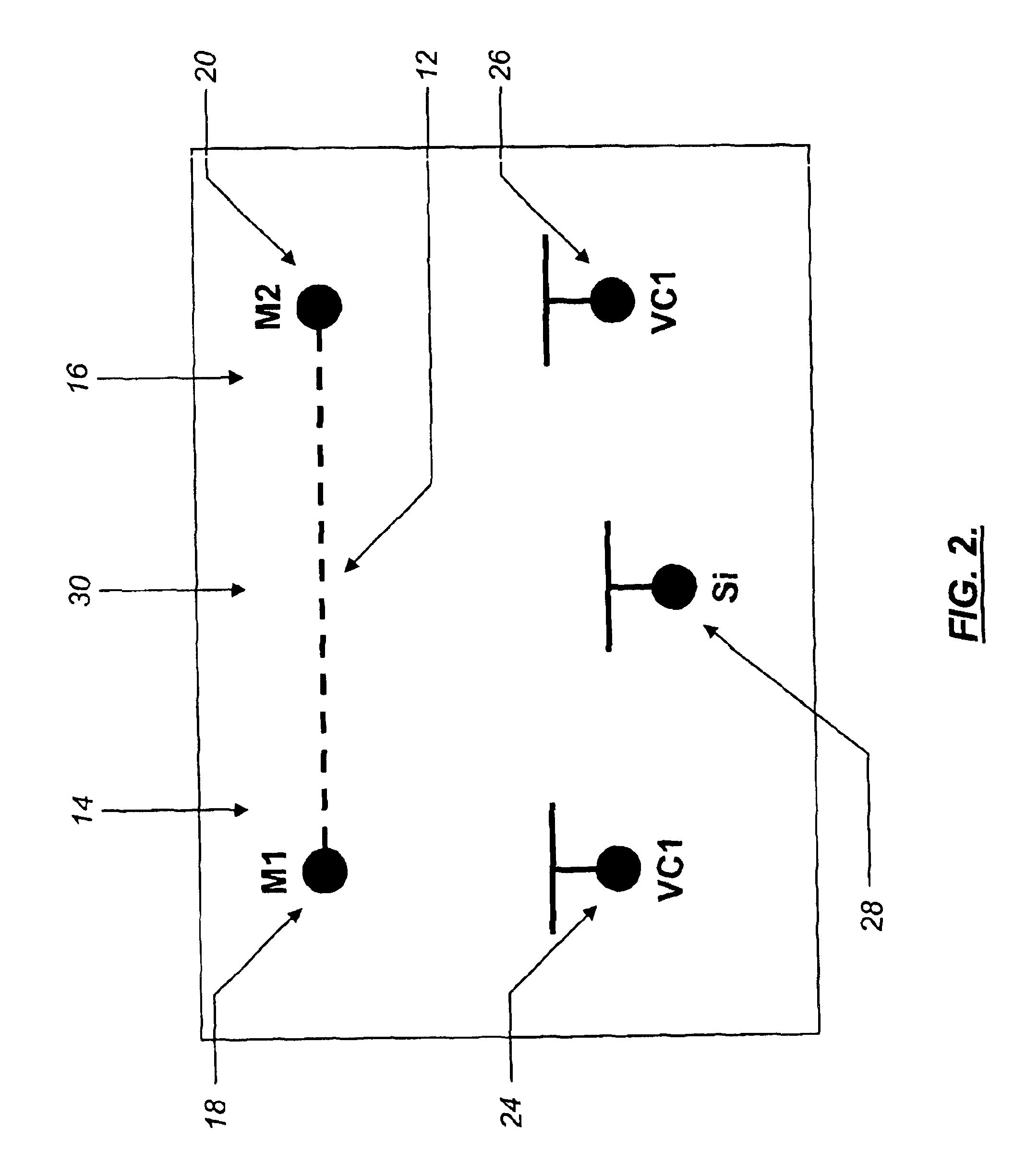
[0017]The present invention provides a method and associated structure for forming an electrostatically-doped carbon nanotube device having well characterized p-type regions and n-type regions, allowing for the creation of nanoscale electronic devices, such as light-emitting diodes (“LEDs”) and the like, with enhanced performance characteristics. More specifically, the present invention provides for the use of a plurality of doping electrodes that are decoupled from a plurality of bias electrodes. Thus, the doping of a carbon nanotube may be finely tuned by varying the bias of each of the plurality of bias electrodes. Advantageously, the method and associated structure of the present invention are capable of providing a carbon nanotube having a P-N junction, a P-I-P junction, a P-I-N junction, an N-I-P junction, an N-I-N junction, a P-N-P junction or an N-P-N junction.

[0018]Referring to FIG. 1, in one embodiment of the present invention, a structure for forming an electrostatically-...


PUM

PropertyMeasurementUnit
distanceaaaaaaaaaa
distanceaaaaaaaaaa
distanceaaaaaaaaaa

Abstract

The present invention provides a method and associated structure for forming an electrostatically-doped carbon nanotube device. The method includes providing a carbon nanotube having a first end and a second end. The method also includes disposing a first metal contact directly adjacent to the first end of the carbon nanotube, wherein the first metal contact is electrically coupled to the first end of the carbon nanotube, and disposing a second metal contact directly adjacent to the second end of the carbon nanotube, wherein the second metal contact is electrically coupled to the second end of the carbon nanotube. The method further includes disposing a first metal electrode adjacent to and at a distance from the first end of the carbon nanotube, wherein the first metal electrode is capacitively coupled to the first end of the carbon nanotube, and disposing a second metal electrode adjacent to and at a distance from the second end of the carbon nanotube, wherein the second metal electrode is capacitively coupled to the second end of the carbon nanotube. The method still further includes selectively applying a first bias to the first metal electrode to electrostatically dope the first end of the carbon nanotube and selectively applying a second bias to the second metal electrode to electrostatically dope the second end of the carbon nanotube.

Description

FIELD OF THE INVENTION[0001]The present invention relates generally to the field of nanotechnology. More specifically, the present invention relates to a method and associated structure for forming an electrostatically-doped carbon nanotube device. The electrostatically-doped carbon nanotube device of the present invention is suitable for use as a light-emitting diode (“LED”), as well as in other applications.BACKGROUND OF THE INVENTION[0002]Carbon nanotubes have attracted a great deal of attention in recent years due to their possibilities for use as nanoscale electronic devices, such as diodes, transistors and semiconductor circuits. Structurally, a carbon nanotube resembles a hexagonal lattice of carbon rolled into a cylinder and may belong to one of two varieties, a single-walled variety and a multi-walled variety. Either of these varieties may, in whole or in part, exhibit the behavior of a metal or a semiconductor material, depending upon their chirality (i.e., conformational ...

Claims


Application Information

Patent Timeline
Patent Type & Authority Patents(United States)
IPC IPC(8): H01L51/05H01L51/30H01L51/40H01L21/00H01L29/12H01L29/26H01L33/24H01L51/00
CPCB82Y10/00B82Y20/00H01L51/0512H01L51/0545H01L51/0048G11C13/025H01L33/24H01L51/002Y10S977/842Y10S977/742Y10S977/95H10K71/30H10K85/221H10K10/462H10K10/466
Inventor LEE, JI UNG
Owner GENERAL ELECTRIC CO
Why Eureka
Try Eureka