Circuit chip connector and method of connecting a circuit chip

a circuit chip and connector technology, applied in the field of interposers, can solve the problems of reducing the accuracy required for placement of ics and silver being an expensive substitute, and achieve the effect of quick and easy attachment of ics

Inactive Publication Date: 2005-05-10
MOTOROLA SOLUTIONS INC
View PDF26 Cites 115 Cited by
  • Summary
  • Abstract
  • Description
  • Claims
  • Application Information

AI Technical Summary

Benefits of technology

[0016]It is a primary objective of the present invention to provide a method for the quick and easy attachment of ICs to a RF antenna, or a similar circuit made from a metallized film substra

Problems solved by technology

The larger area of the interposer pads reduces the accuracy required for placement of ICs during manufacture while still providing effective electrical

Method used


Image

  • Circuit chip connector and method of connecting a circuit chip
  • Circuit chip connector and method of connecting a circuit chip
  • Circuit chip connector and method of connecting a circuit chip

Examples


Embodiment Construction

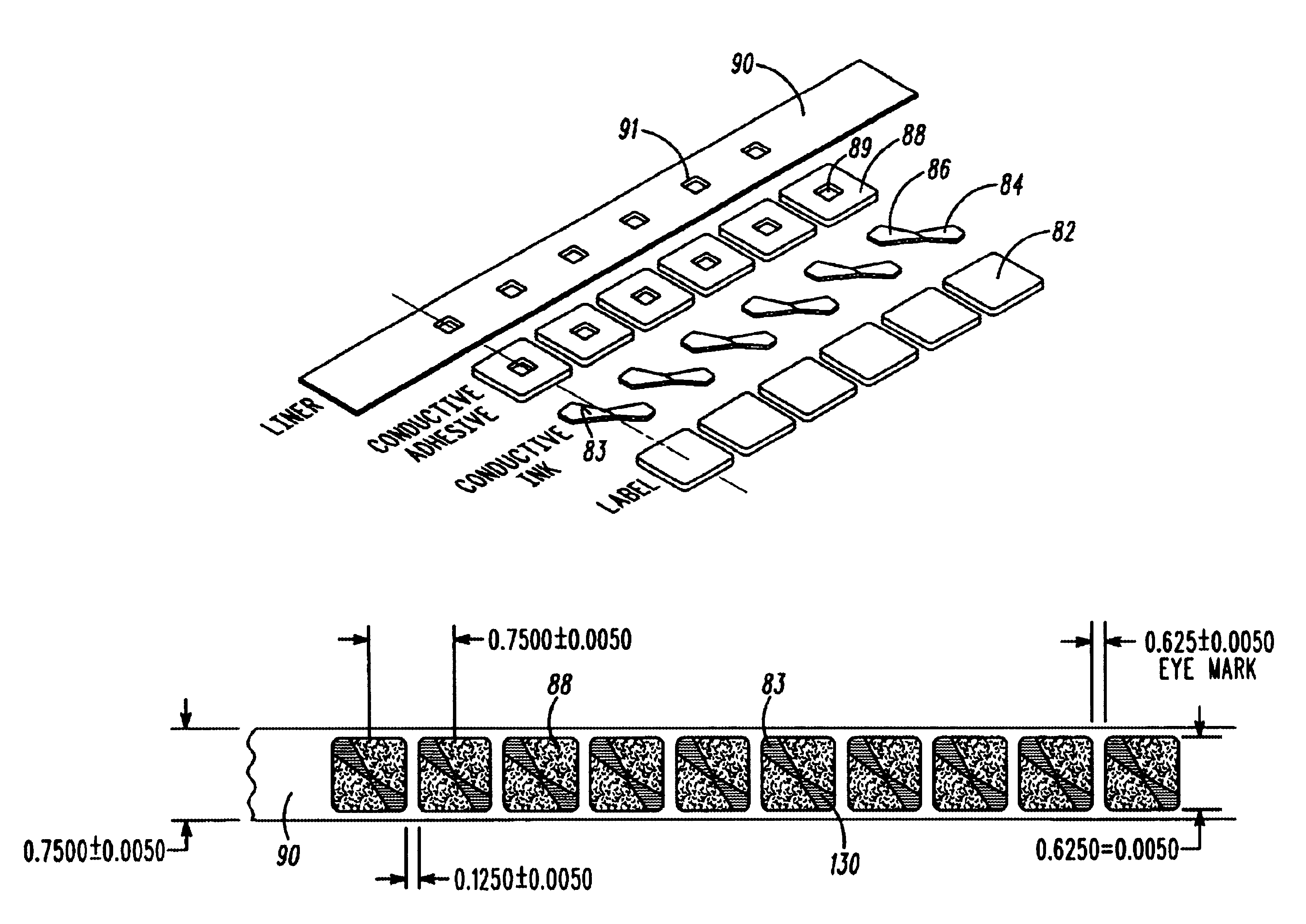
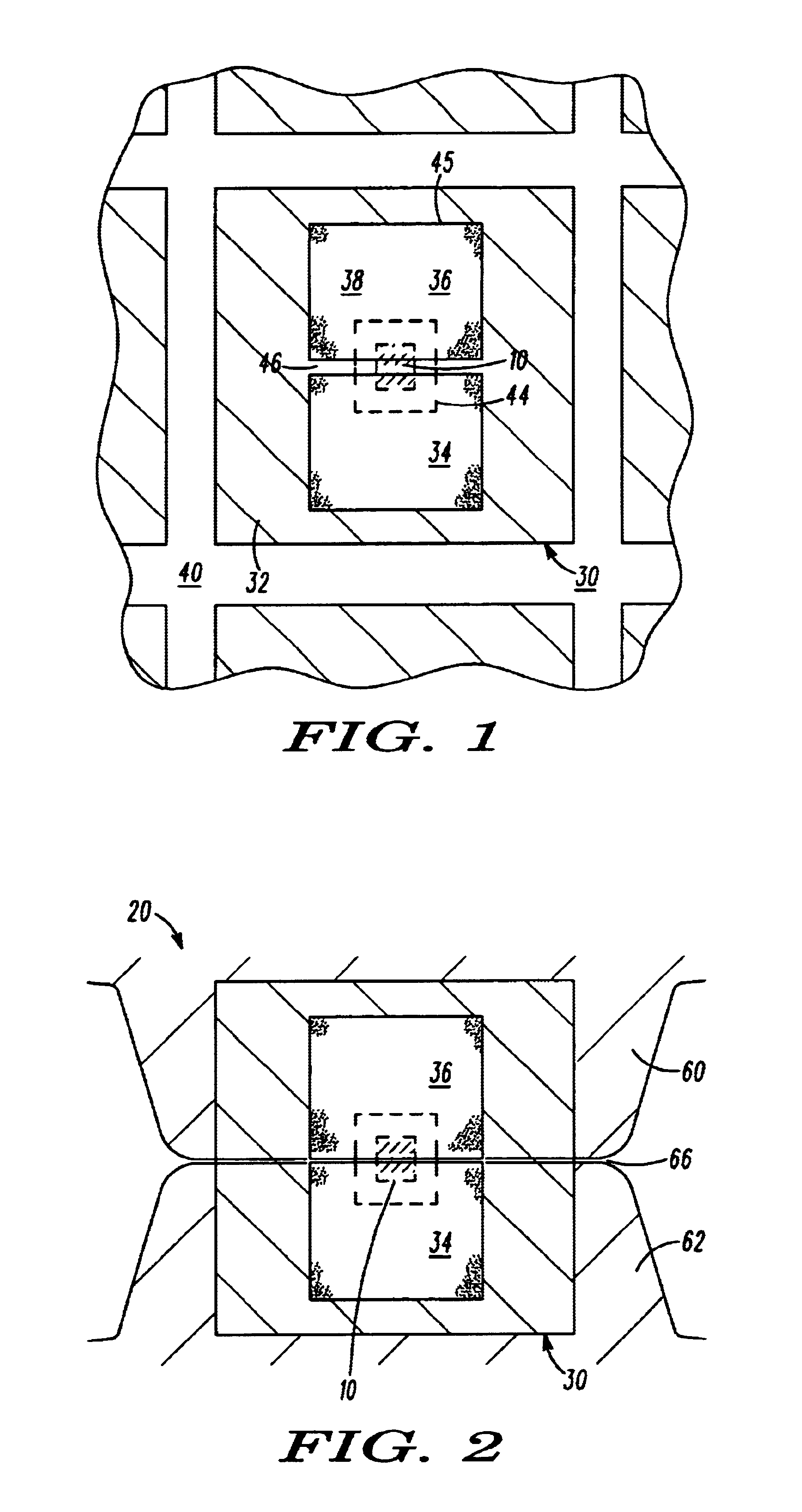
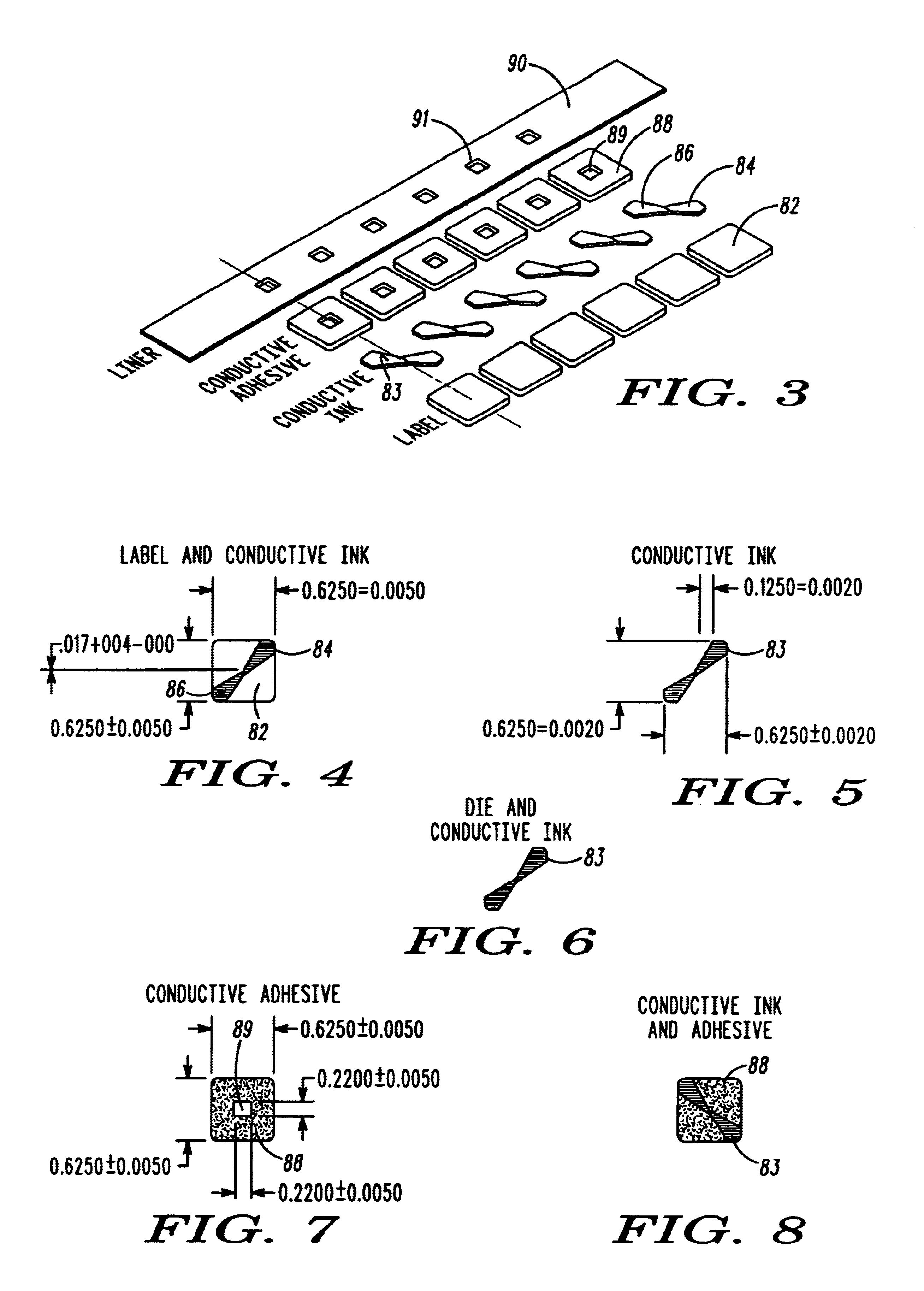
[0037]A thin film circuit, shown as an antenna 20 (or a similar circuit made from metallized film or other metallized flex circuit) can be made from a thin etched or stamped foil, typically manufactured from a thin foil of copper, copper-alloy, or nickel-iron alloy by stamping or etching. The etching or stamping creates patterns on strips that become antennas. Other methods of making an antenna include printing a conductive ink. This invention relates to ICs 10, which are joined and electrically connected to individual antennas 20, focusing on the interposer 30, its substrate 32, and the printing of contact pads 34 and 36 thereon onto which the IC 10 is incorporated. The layer of anisotropically conductive pressure sensitive adhesive 38 makes contact with connectors of the IC 10 as to interconnect the antenna 20 and the IC 10. Pressure sensitive adhesives are selected for ease of application, but other adhesives are available though not necessarily preferred. Two different adhesives...


PUM


Abstract

A radio frequency identification tag comprising a first substrate and a second substrate is disclosed. An antenna element is disposed on the first substrate, and a first contact pad and a second contact pad is disposed on the second substrate. A circuit is coupled to the first and second contact pads, and the first and second contact pads are designed to make electrical contact with the antenna element.

Description

RELATED U.S. APPLICATION DATA[0001]This application has partial priority to U.S. Provisional Application Ser. No. 60 / 125,842, filed Mar. 24, 1999 and U.S. Provisional Application Ser. No. 60 / 149,486, filed Aug. 18, 1999.BACKGROUND OF THE INVENTION[0002]The present invention relates to interposers and a method of mounting an integrated circuit chip (IC) or similar device using such an interposer connected across a gap between thin film circuits, such as two conductive film sections of a conductive film antenna, or similar circuit made from conductive film or other conductive flex circuit. More specifically, the invention is directed toward a method of mass-producing devices, such as radio frequency identification tags (RFIDs), by mounting integrated circuit chips (ICs) on interposers that are then physically and electrically connected to the circuit, such as a conductive film antenna, using a pressure sensitive conductive adhesive.[0003]Radio frequency (RF) devices such as RFIDs can ...

Claims


Application Information

Patent Timeline
IPC IPC(8): H01L21/02H01L21/60H01L23/48H01L23/498G06K19/077
CPCG06K19/07749G06K19/07758G06K19/07786H01L23/49827H01L23/49855H01L24/83H01L24/29G06K19/07752H01L2924/00013H01L2224/29011H01L2224/8319H01L2224/838H01L2224/83851H01L2924/01005H01L2924/01013H01L2924/01029H01L2924/01047H01L2924/01075H01L2924/01082H01L2924/0781H01L2924/14H01L2224/2919H01L2924/01006H01L2924/01033H01L2924/014H01L2924/0665H01L2224/29101H01L2224/293H01L2224/2929H01L2924/00H01L2924/00014H01L2224/29099H01L2224/29199H01L2224/29299H01L2924/12042
Inventor PENNAZ, THOMAS J.EBERHARDT, NOEL H.
Owner MOTOROLA SOLUTIONS INC
Why Eureka
Try Eureka