Lithographic apparatus and device manufacturing method

a technology of lithographic apparatus and manufacturing method, which is applied in the direction of printers, dynamo-electric machines, instruments, etc., can solve the problems of increasing the mass of the actuator, reducing the accuracy of its performance, and damage to components within the apparatus or the substrate, so as to improve the heat transfer characteristics

Inactive Publication Date: 2005-05-10
ASML NETHERLANDS BV
View PDF9 Cites 20 Cited by
  • Summary
  • Abstract
  • Description
  • Claims
  • Application Information

AI Technical Summary

Benefits of technology

[0016]It is an object of the present invention to provide a coil for an actuator or positioning device for use in a lithographic projection apparatus that has improved heat transfer characteristics.

Problems solved by technology

Temperature changes and temperature gradients within the lithographic apparatus reduce the accuracy of its performance and thermal strains may cause damage to components within the apparatus or the substrates being processed by the apparatus.
However this increases the mass of the actuator, resulting in larger required forces and more heat generated.
However, with conventional coil designs made up of orthocyclically wound wire, the heat transmission through the coil is low.
Each insulated piece of wire is only in line-contact with the adjacent pieces of wire, limiting the area across which heat may be conducted.
Furthermore, the material 13 used to electrically insulate the wires 11 from one another tends to be a poor conductor of heat further reducing the heat transfer characteristic across the coil as a whole.

Method used


Image

  • Lithographic apparatus and device manufacturing method
  • Lithographic apparatus and device manufacturing method
  • Lithographic apparatus and device manufacturing method

Examples


embodiment 1

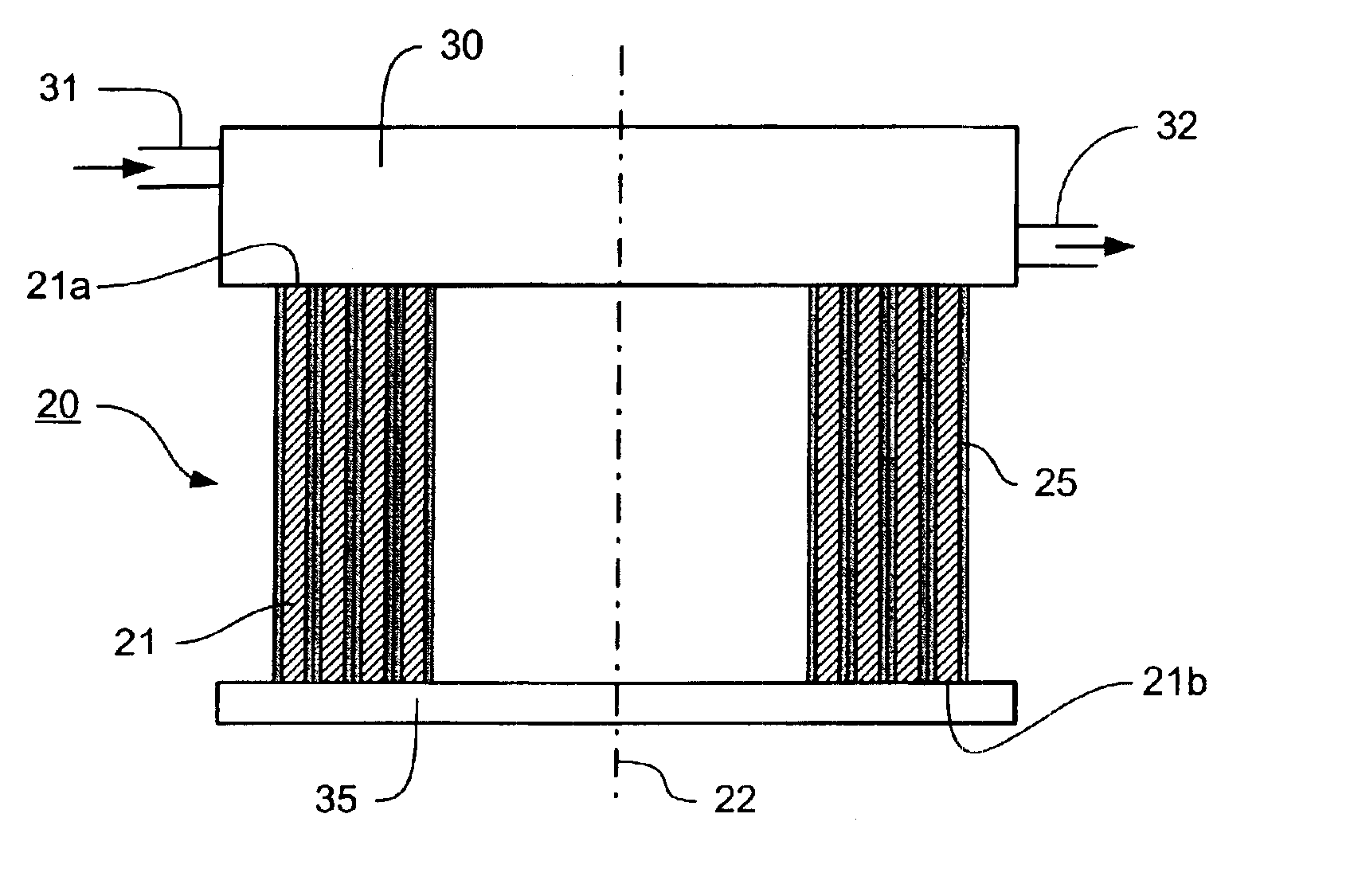
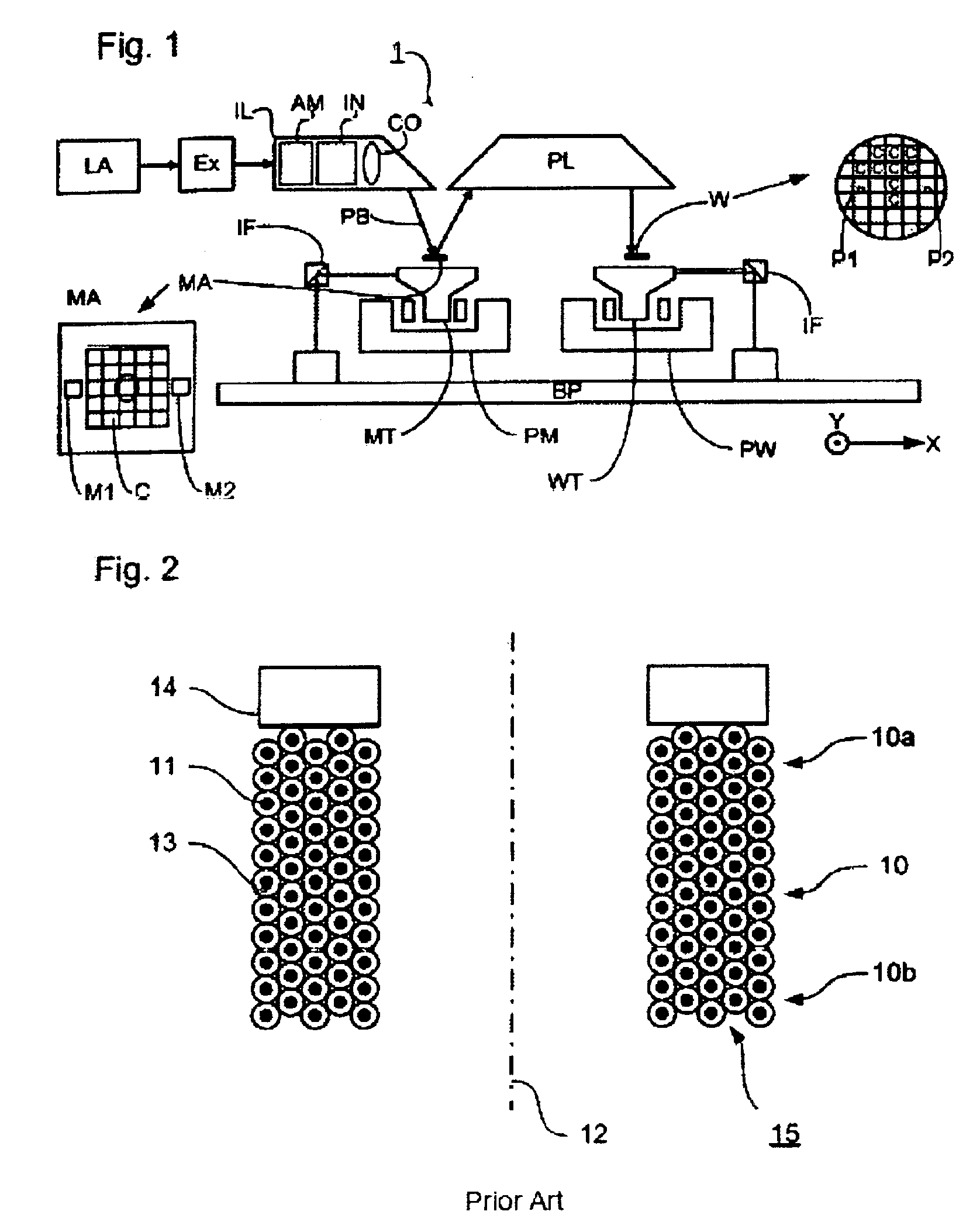
[0043]FIG. 1 schematically depicts a lithographic projection apparatus according to a particular embodiment of the invention. The apparatus comprises:[0044]a radiation system Ex, IL, for supplying a projection beam PB of radiation (e.g. EUV radiation), which in this particular case also comprises a radiation source LA;[0045]a first object table (mask table) MT provided with a mask holder for holding a mask MA (e.g. a reticle), and connected to first positioning means for accurately positioning the mask with respect to item PL;[0046]a second object table (substrate table) WT provided with a substrate holder for holding a substrate W (e.g. a resist-coated silicon wafer), and connected to second positioning means for accurately positioning the substrate with respect to item PL;[0047]a projection system (“lens”) PL (e.g. mirror group) for imaging an irradiated portion of the mask MA onto a target portion C (e.g. comprising one or more dies) of the substrate W.

[0048]As here depicted, the...


PUM

PropertyMeasurementUnit
thicknessaaaaaaaaaa
thicknessaaaaaaaaaa
thicknessaaaaaaaaaa

Abstract

A coil for use in an actuator in a lithographic projection apparatus. The coil is formed of a strip of electrically conducting sheet-material that is wound round a winding axis. Respective turns of the strip of sheet-material are separated by an electrically non-conducting layer.

Description

[0001]This application claims priority to European Application No. 02254101.5, filed Jun. 12, 2002.BACKGROUND OF THE INVENTION[0002]1. Field of the Invention[0003]The present invention relates generally to a lithographic projection apparatus and more particularly to a lithographic projection apparatus including electromagnetic actuators.[0004]2. Description of the Related Art[0005]The term “patterning means” or “patterning structure” as here employed should be broadly interpreted as referring to means that can be used to endow an incoming radiation beam with a patterned cross-section, corresponding to a pattern that is to be created in a target portion of the substrate; the term “light valve” can also be used in this context. Generally, the pattern will correspond to a particular functional layer in a device being created in the target portion, such as an integrated circuit or other device (see below). Examples of such patterning means include:[0006]A mask. The concept of a mask is ...

Claims


Application Information

Patent Timeline
Patent Type & Authority Patents(United States)
IPC IPC(8): G03F7/20H02K41/03H02K3/18H02K3/32H01L21/027
CPCG03F7/70758H02K3/18H02K41/031H02K41/03H02K2201/18H02K3/325H01L21/027
Inventor FRISSEN, PETRUS CAROLUS MARIACOMPTER, JOHAN CORNELISTABOR, ROB
Owner ASML NETHERLANDS BV
Why Eureka
Try Eureka