Fast parallel cascaded array modular multiplier

a cascaded array and modular multiplier technology, applied in the field of digital signal processing, can solve the problems of slow hardware approach to modular multiplication, limited success in scaling beyond the level of a single linear array, and performance scale only logarithmically with respect, so as to achieve optimal systolic clock rate, fast parallel processing of modular multiplication, and reduced number of internal signal buses in the integrated circuit implementation

Inactive Publication Date: 2005-05-10
FREKING WILLIAM L
View PDF5 Cites 5 Cited by
  • Summary
  • Abstract
  • Description
  • Claims
  • Application Information

AI Technical Summary

Benefits of technology

[0012]The primary object of this invention is fast parallel processing of modular multiplication.
[0013]It is an advantage of this invention that multiple independent data streams may be simultaneously processed. The number of data streams is arbitrary, limited only by implementation area.
[0014]It is a primary advantage of this method that throughput performance scales linearly with the area of the integrated circuit implementation while maintaining the optimal systolic clock rate. The latter is attained through guaranteeing properties of purely nearest neighbor interconnections between processing elements and unit signal fan out.
[0015]It is an advantage of this invention that input and output data share signal lines such that the number of internal signal buses in an integrated circuit implementation are reduced.
[0016]It is an advantage of this invention that a unified control unit may be utilized when the modular multiplier unit is used in a modular exponentiator.

Problems solved by technology

Since large word lengths on the order of thousands of bits are typically processed, hardware approaches to modular multiplication are typically very slow.
However, efforts to scale the performance beyond the level offered by a single linear array have encountered very limited success.
However, performance scales only logarithmically with respect to consumed integrated circuit area.
However, the clock rate is severely limited by the required full-word-length signal broadcasts of the modular correction selection bit.
Implementational efforts to increase the signal drive through transistor sizing destroys the linear performance-area trade off and only provide minor mitigation of the slow-clock-rate obstacle plaguing this methodology.

Method used


Image

  • Fast parallel cascaded array modular multiplier
  • Fast parallel cascaded array modular multiplier

Examples


Embodiment Construction

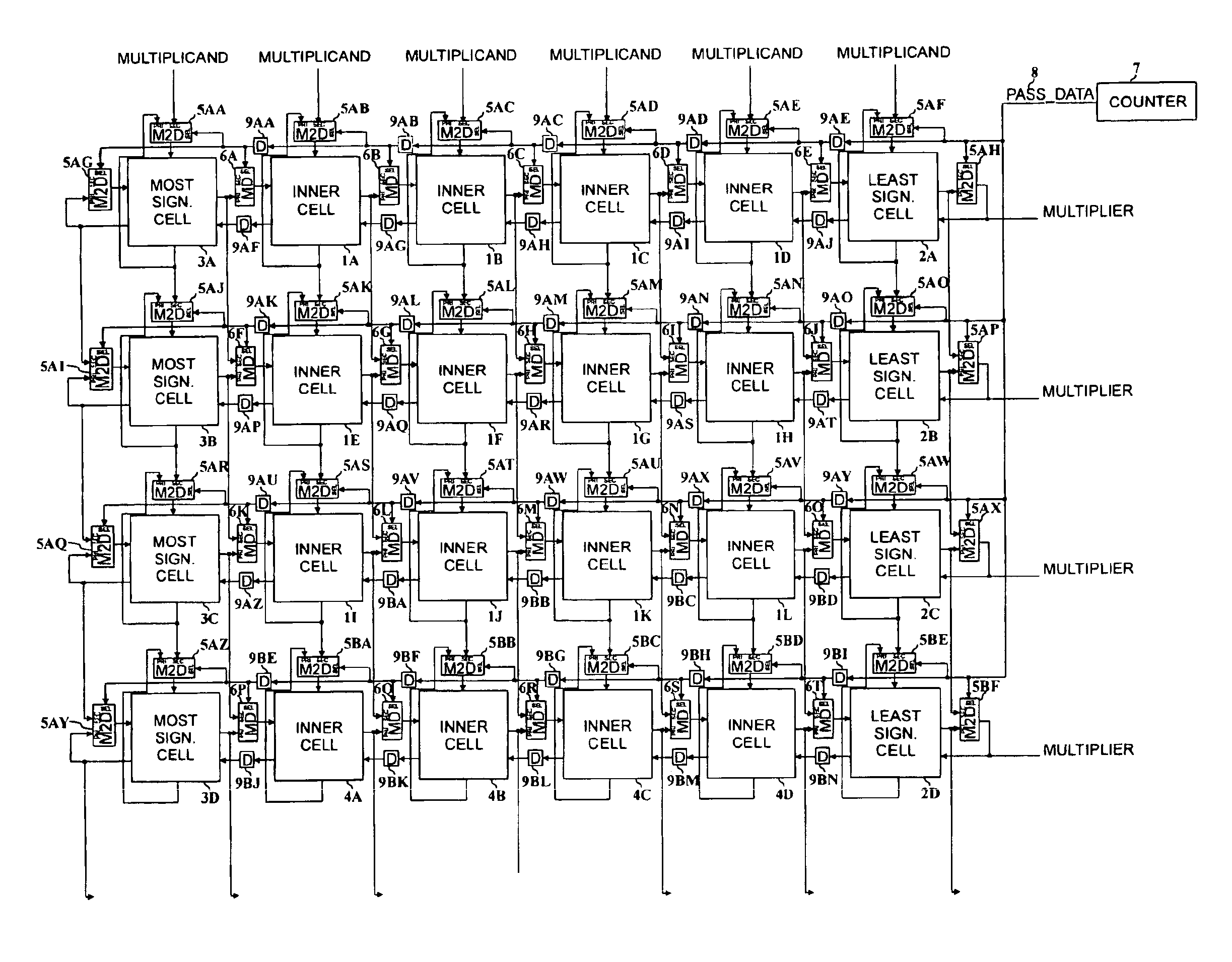
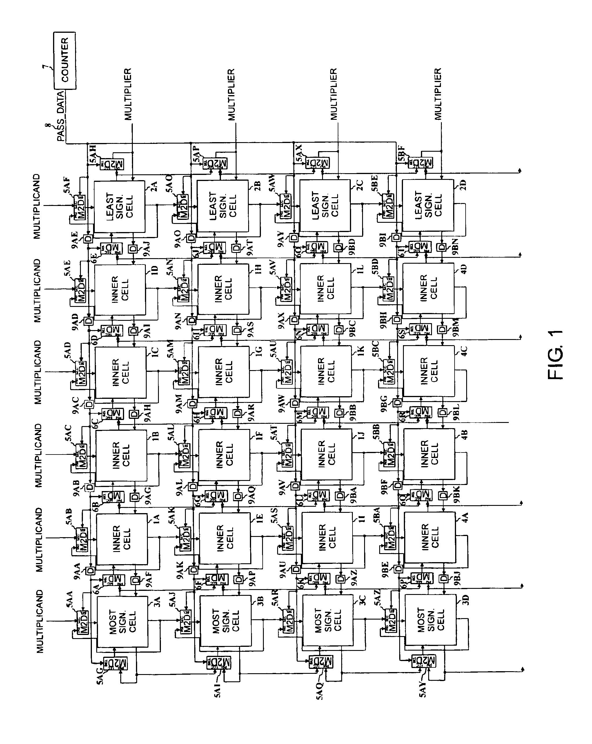
[0018]The preferred embodiment is delineated in FIG. 1. It consists of a cascade of K linear systolic arrays of bit-wise processing cells, where K is chosen according to the amount of integrated circuit area available for the implementation. The value of K directly relates to the amount of parallelism implemented in the system. Each array is composed of N+1 cells, where N represents the word length of the modulus value in bits.

[0019]Each cell possesses a set of bit-wise inputs corresponding to the multiplicand, multiplier, modular correction, modular selection, partial sum, and two previous carry signals. Each cell also possesses a set of bit-wise outputs corresponding to the multiplicand, multiplier, modular correction, modular selection, generated partial sum, and two generated carry signals. Each inner cell 1 excluding the leftmost and rightmost peripheral cells in each array and all cells in the bottommost array, is interconnected within the structure in the following manner. Th...


PUM


Abstract

A fast, parallel modular multiplier is presented which is scalable according to available hardware resources. Linear throughput increases with respect to consumed resources is achieved. Multiple independent data streams may be processed simultaneously, and optimal clock rates are attained by virtue of limited fan-out of all signal paths and nearest neighbor interconnections. Integrated circuit implementation is benefited by the potential for signal sharing among input and output busses and a common control interface for all independent data streams.

Description

CROSS-REFERENCE TO RELATED APPLICATIONS[0001]Not applicable.BACKGROUND OF THE INVENTION[0002]1. Field of the Invention[0003]The present invention relates to the processing of digital signals to render modular multiplication.[0004]2. Description of Related Art[0005]Modular multiplication, which is the computation of A·B modulo M where A, B, and M are integer values, is a fundamental mathematical operation in applications based on number-theoretic arithmetic. A central application area is cryptography, where techniques such as the popular RSA and DSS methods utilize modular multiplication as the elemental computation. Since large word lengths on the order of thousands of bits are typically processed, hardware approaches to modular multiplication are typically very slow. Existing art attempts to address this deficiency through a handful of approaches.[0006]Linear systolic array approaches dominate the art, with the article C. Walter, “Systolic modular multiplication,” IEEE Transactions...

Claims


Application Information

Patent Timeline
Patent Type & Authority Patents(United States)
IPC IPC(8): G06F7/72G06F7/60G06F7/52G06F7/48
CPCG06F7/722
Inventor FREKING, WILLIAM L.PARHI, KESHAB K. P
Owner FREKING WILLIAM L
Why Eureka
Try Eureka