

Bipolar transistors with low-resistance emitter contacts
a bipolar transistor and emitter contact technology, applied in the field of integrated circuits, to achieve the effect of reducing resistance, superior switching speed and current gain
- Summary
- Abstract
- Description
- Claims
- Application Information
AI Technical Summary
Benefits of technology
Problems solved by technology
Method used
Image

Examples
Embodiment Construction
[0017]The following detailed description, which references and incorporates FIGS. 1-7, describes and illustrates specific embodiments of the invention. These embodiments, offered not to limit but only to exemplify and teach the invention, are shown and described in sufficient detail to enable those skilled in the art to practice the invention. Thus, where appropriate to avoid obscuring the invention, the description may omit certain information known to those of skill in the art.
Exemplary Fabrication Method and Structure for Bipolar Transistor with Low-Resistance Emitter Contact
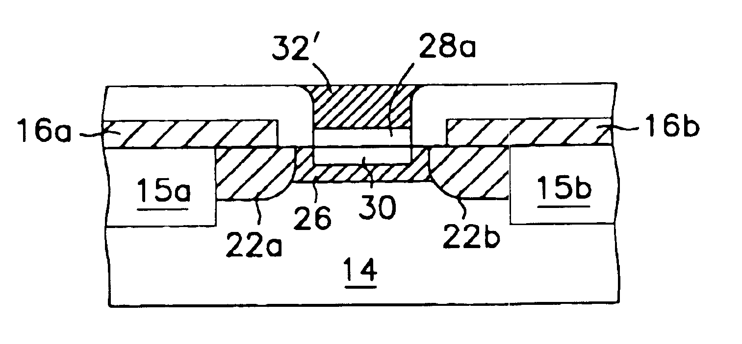
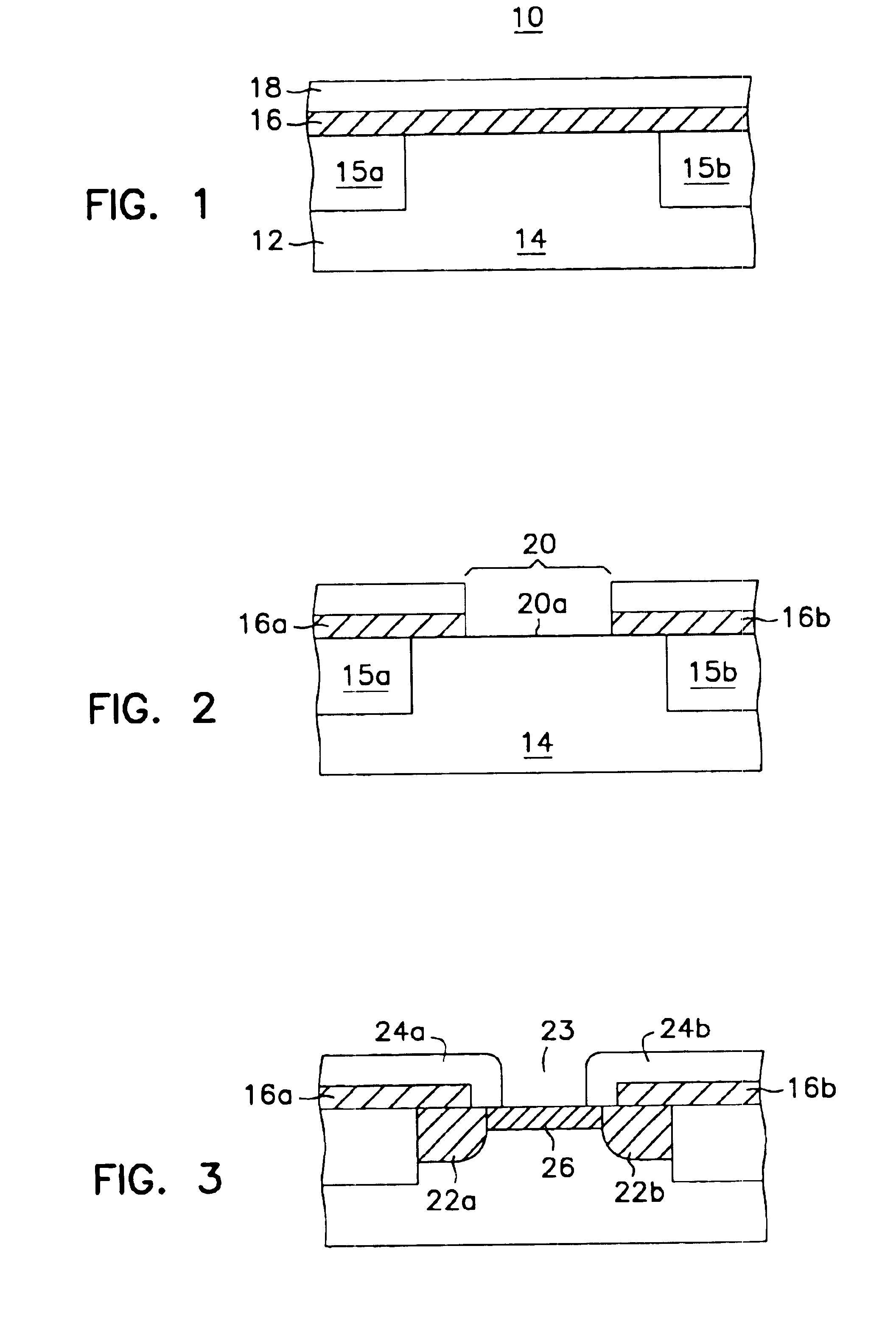
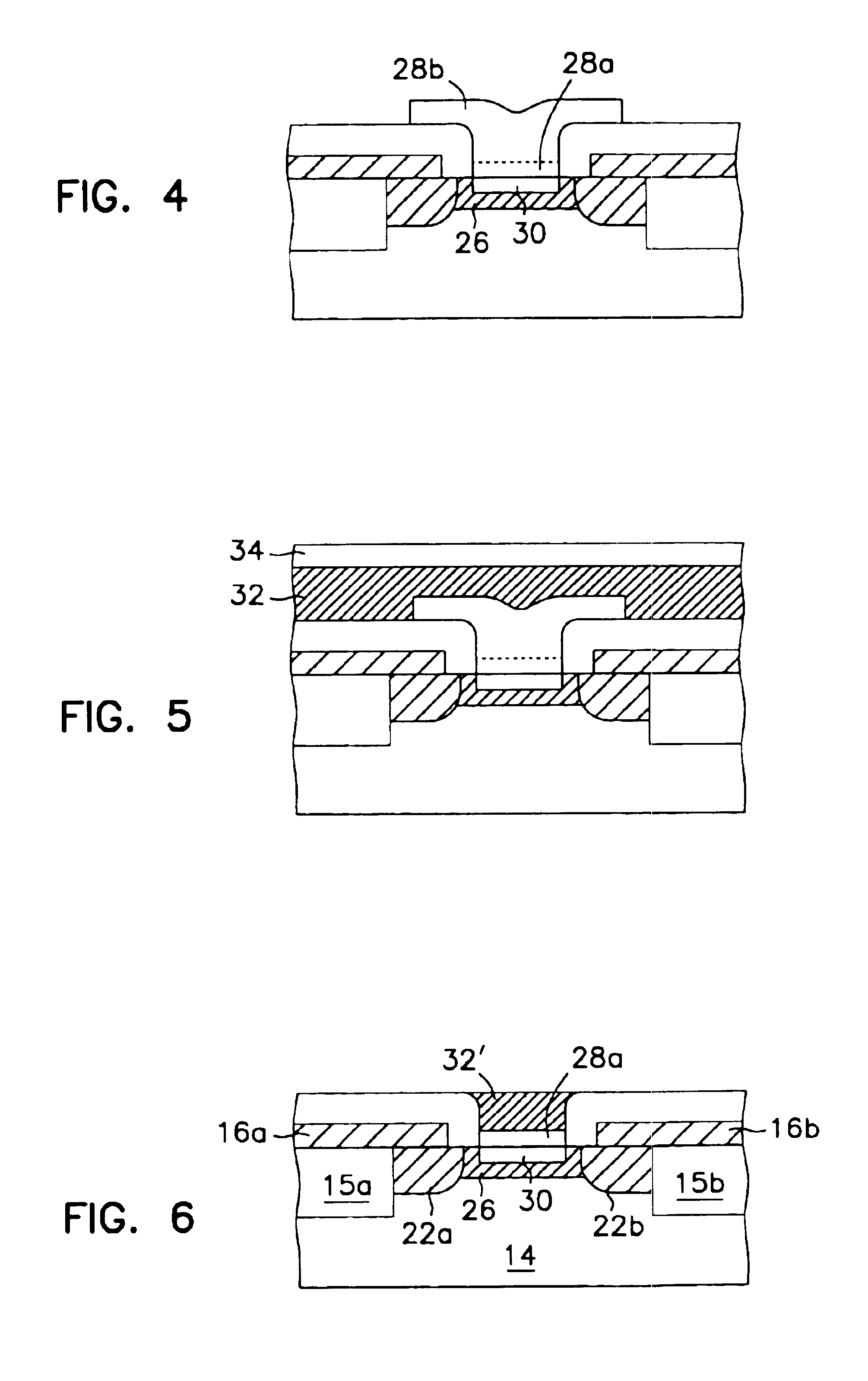
[0018]FIGS. 1-6 show a number of exemplary integrated-circuit assemblies, which taken collectively and sequentially illustrate the exemplary method of making a bipolar transistor with a low-resistance emitter contact. In particular, FIGS. 1-3 depict part of a conventional method of making a standard double-polysilicon, self-aligned bipolar transistor, and FIGS. 4-6 illustrate an extension to the process that ...
PUM
 Abstract
Description
Claims
Application Information