Capped dual metal gate transistors for CMOS process and method for making the same

a metal gate transistor and cmos technology, applied in the field of semiconductor fabrication, can solve the problems of increasing the difficulty of incorporating polysilicon gates into advanced technologies, increasing the difficulty of polysilicon gate use, and increasing the difficulty of reducing the thickness of dielectrics

Inactive Publication Date: 2005-05-17
NXP USA INC
View PDF16 Cites 70 Cited by
  • Summary
  • Abstract
  • Description
  • Claims
  • Application Information

AI Technical Summary

Problems solved by technology

The use of polysilicon gate structures is becoming unfeasible as gate dielectric thicknesses steadily decrease.
More specifically, boron diffusion from p-type polysilicon gates into the transistor channel and poly depletion effects associated with devices having low thermal budget and thin gate oxides are making it increasingly difficult to incorporate polysilicon gates into advanced technologies.
In addition, as semiconductor processing moves away from the use

Method used


Image

  • Capped dual metal gate transistors for CMOS process and method for making the same
  • Capped dual metal gate transistors for CMOS process and method for making the same
  • Capped dual metal gate transistors for CMOS process and method for making the same

Examples


Embodiment Construction

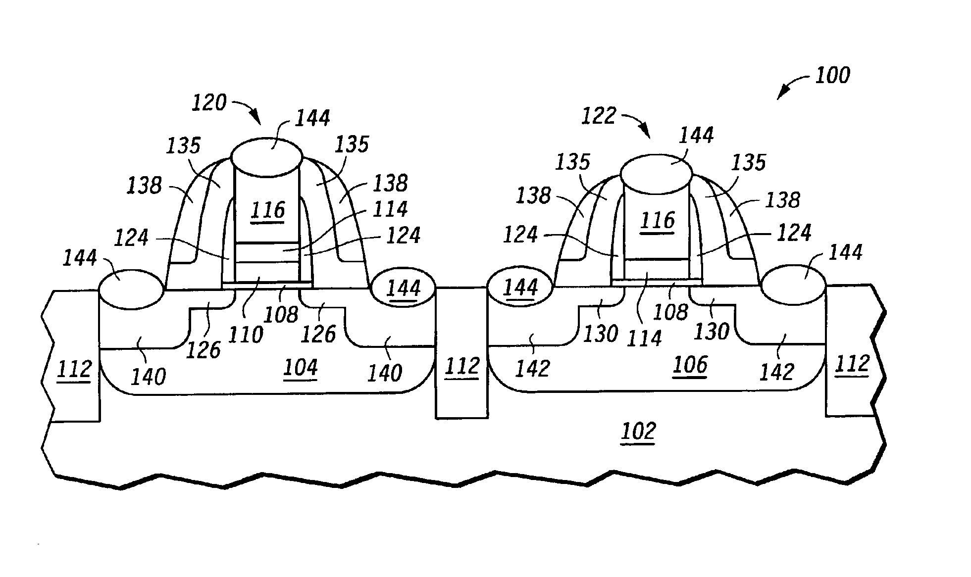
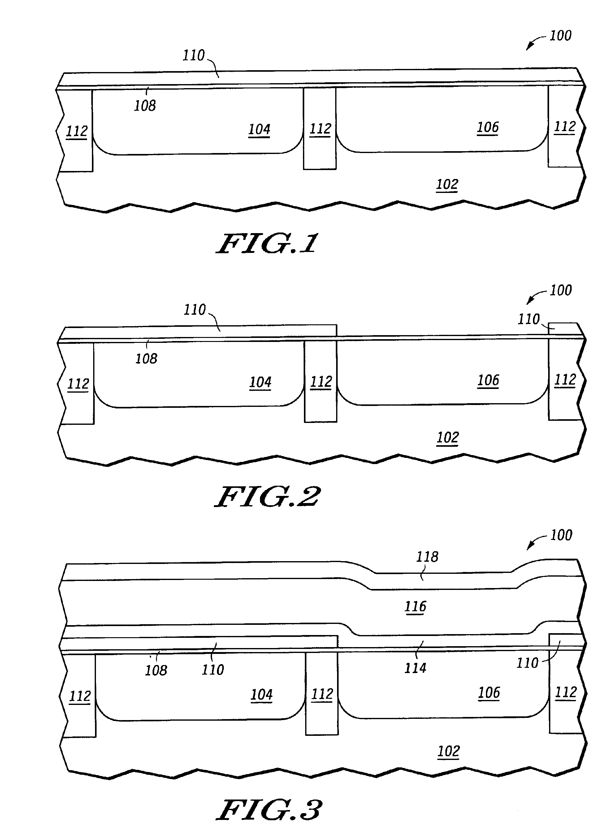
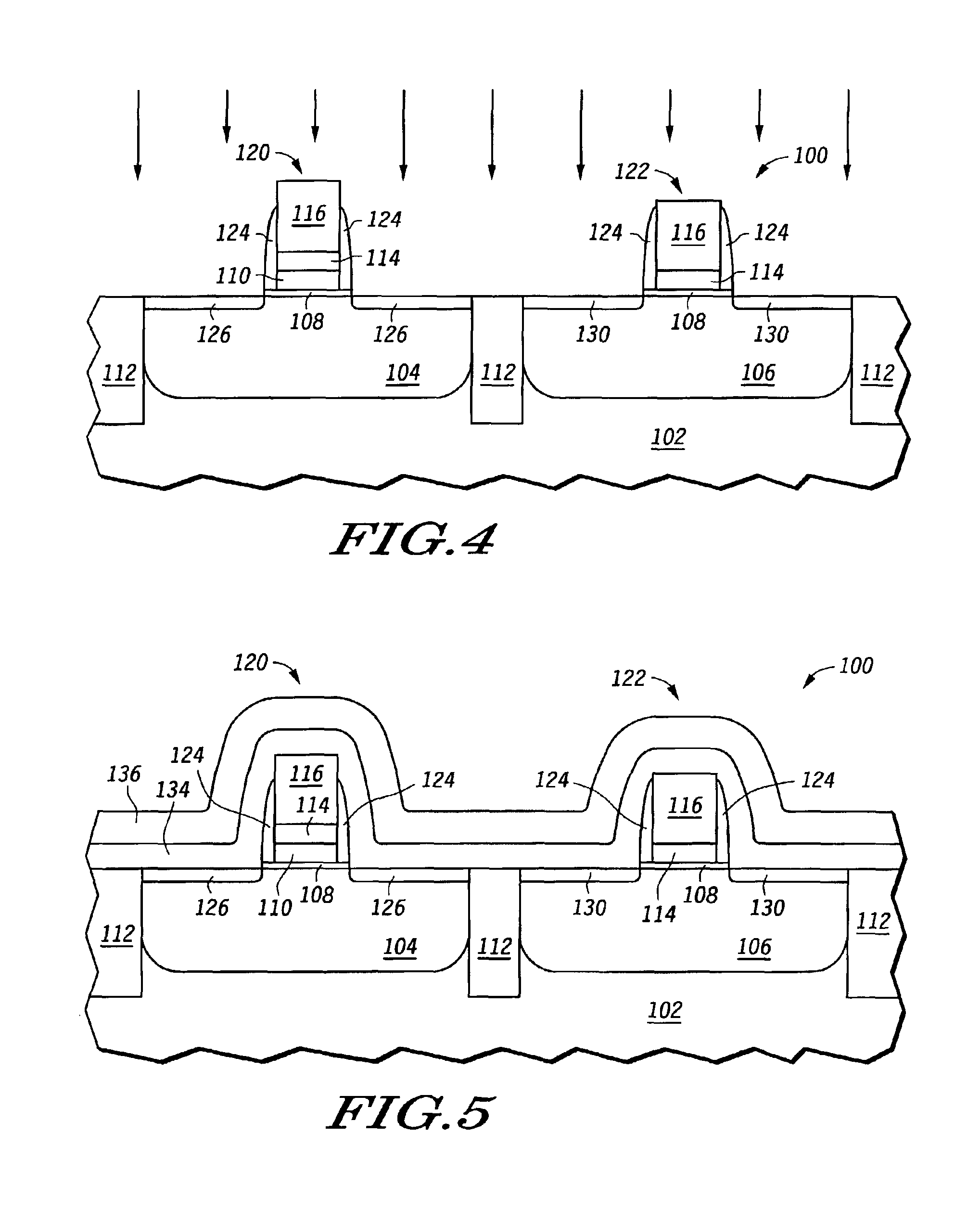
[0016]Generally, the present invention overcomes the previously described problem of etchant attacks on dual metal gate structures through a combination of spacers and a polysilicon capping layer. Thin, “zero spacers”, preferably of silicon nitride, are formed immediately adjacent the patterned gate structures in each of the PMOS and NMOS portions of the device. The extension implants, and halo implants if used, are then performed. The zero spacers protect the sides of the gate structure during removal of the photoresist mask used to mask the implants. A polysilicon capping layer is used to protect the top of the gate structures. Polysilicon is not attacked by conventional pirhana or SC-1 cleans.

[0017]The polysilicon capping layer was also found to be beneficial in protecting the sides of the gate structure. A problem discovered by Applicants in using zero layer spacers alone, or zero layer spacers in conjunction with an overlying ARC (anti-reflective coating) on the gates, is that ...


PUM


Abstract

A first gate (120) and a second gate (122) are preferably PMOS and NMOS transistors, respectively, formed in an n-type well (104) and a p-type well (106). In a preferred embodiment first gate (120) includes a first metal layer (110) of titanium nitride on a gate dielectric (108), a second metal layer (114) of tantalum silicon nitride and a silicon containing layer (116) of polysilicon. Second gate (122) includes second metal layer (114) of a tantalum silicon nitride layer on the gate dielectric (108) and a silicon containing layer (116) of polysilicon. First spacers (124) are formed adjacent the sidewalls of the gates to protect the metals from chemistries used to remove photoresist masks during implant steps. Since the chemistries used are selective to polysilicon, the spacers (124) need not protect the polysilicon capping layers, thereby increasing the process margin of the spacer etch process. The polysilicon cap also facilitates silicidation of the gates.

Description

CROSS-REFERENCE TO RELATED APPLICATION[0001]The present application is related to a commonly assigned, co-pending application by Madhukar et al. entitled, “Dual Metal Gate Transistors for CMOS Process,” filed Jun. 12, 2000 as U.S. Ser. No. 09 / 592,448; and to a commonly assigned, co-pending application by Ngai et al. entitled, “Semiconductor Device and a Method Therefor,” filed May 26, 2001 as U.S. Ser. No. 09 / 865,855.FIELD OF THE INVENTION[0002]The present invention is related to the field of semiconductor fabrication and more particularly to a fabrication process incorporating differing gate metals for NMOS (n-channel metal oxide semiconductor) and PMOS (p-channel MOS) devices.RELATED ART[0003]In the field of semiconductor fabrication, it is typically desirable to fabricate n-channel and p-channel transistors with matching threshold voltages. In addition, it is desirable if the absolute value of the n-channel and p-channel threshold voltages are close to zero to increase the device...

Claims


Application Information

Patent Timeline
IPC IPC(8): H01L21/70H01L21/8238
CPCH01L21/823814H01L21/823864H01L21/823842H01L21/823835
Inventor SAMAVEDAM, SRIKANTH B.TOBIN, PHILIP J.
Owner NXP USA INC
Why Eureka
Try Eureka