Inductor having small energy loss

Inactive Publication Date: 2005-05-17
MITSUBISHI ELECTRIC CORP
View PDF2 Cites 34 Cited by
  • Summary
  • Abstract
  • Description
  • Claims
  • Application Information

AI Technical Summary

Benefits of technology

[0012]It is an object of the present invention to provide an i

Problems solved by technology

In addition, energy loss is large in an integrated circuit including such a spiral inductor as a whole since energy loss in the spiral inductor is large.
However, an inductor described in JP Laid-Ope

Method used


Image

  • Inductor having small energy loss
  • Inductor having small energy loss
  • Inductor having small energy loss

Examples


Example

(First Embodiment)

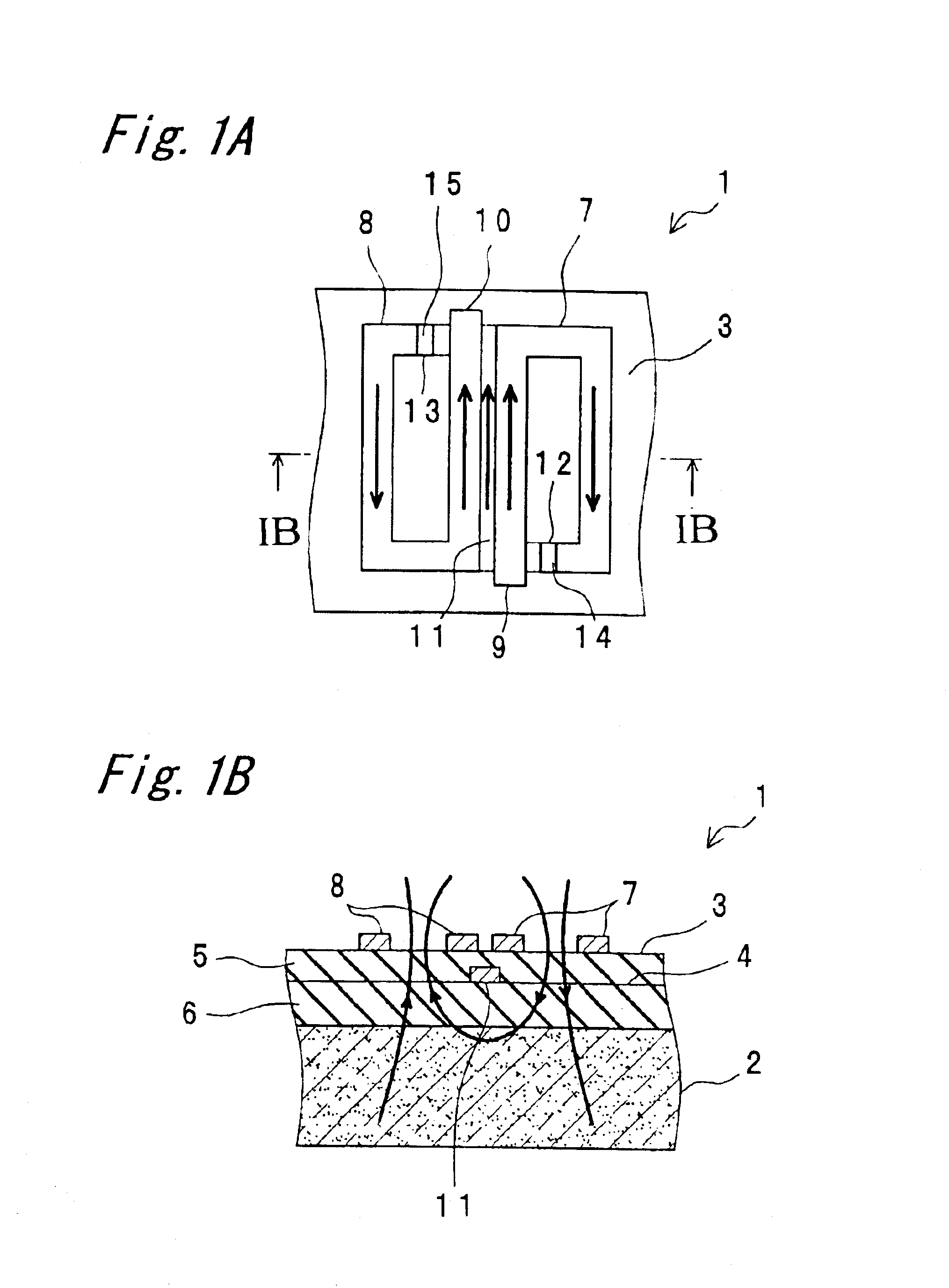
[0027]FIGS. 1A and 1B show a spiral inductor according to the first embodiment of the present invention, in which FIG. 1A is a plan view of the spiral inductor, and FIG. 1B is a sectional view taken along line IB—IB in FIG. 1A. The spiral inductor 1 has a laminated structure in which a wiring layer and an insulating layer are layered alternately on a semiconductor substrate 2. Referring to FIG. 1B, the laminated structure has wiring layers 3 and 4, an insulating layer 5 interposed between them and an insulating layer 6 interposed between the wiring layer 4 and the semiconductor substrate 2. More specifically, the insulating layer 6, the wiring layer 4, the insulating layer 5 and the wiring layer 3 are layered on the semiconductor substrate 2 in this order. Each of the wiring layers in the spiral inductor 1 has an electrically conductive pattern made of aluminum (Al), copper (Cu) or the like. As shown in FIG. 1A, the spiral inductor 1 includes first and second windi...

Example

(Second Embodiment)

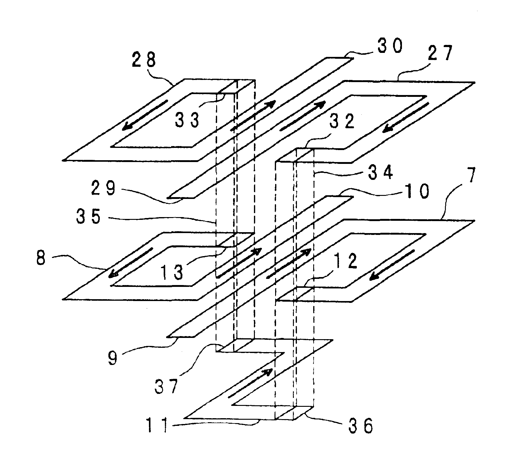
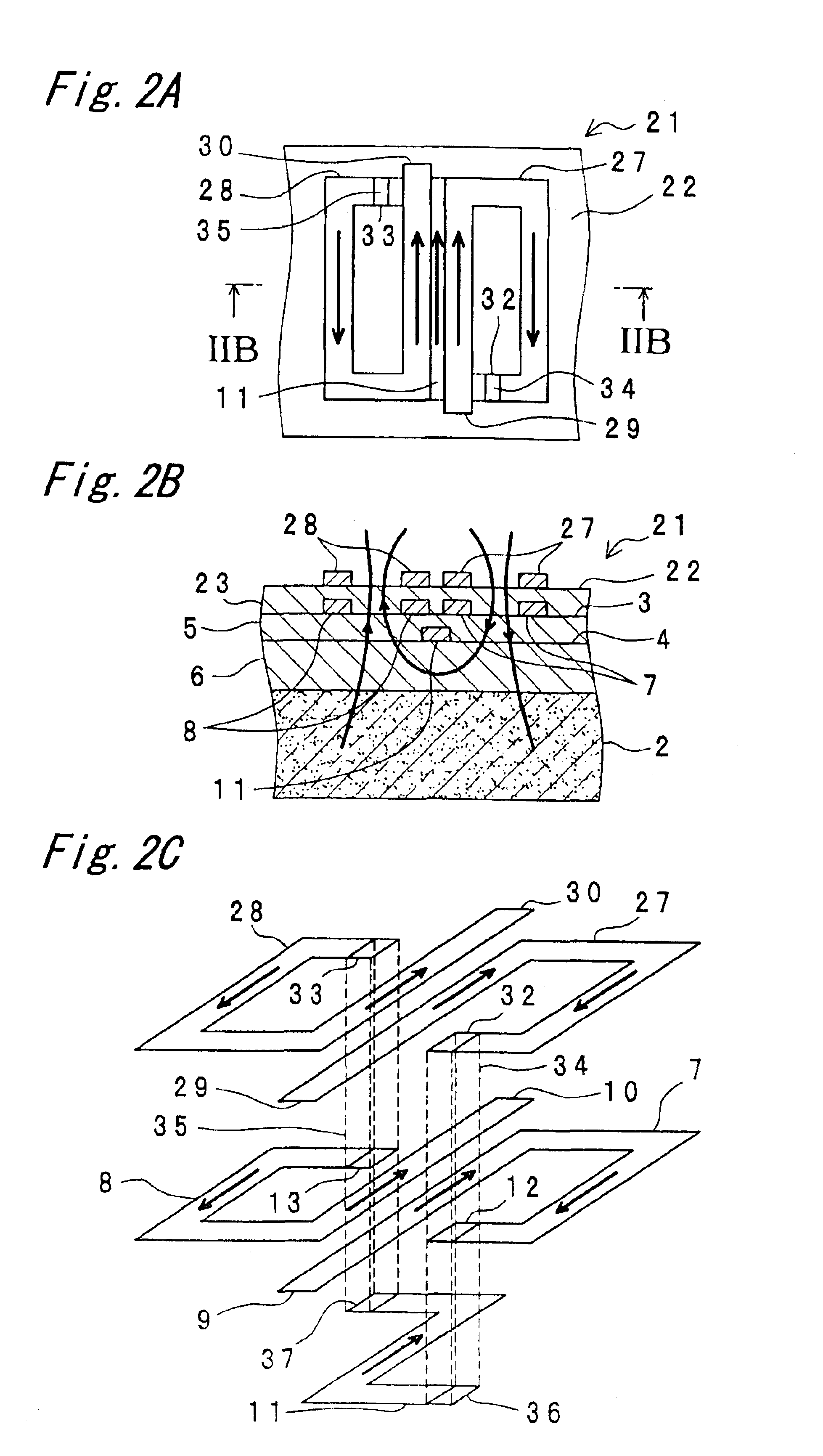
[0040]FIGS. 2A and 2B show a spiral inductor according to the second embodiment of the present invention. FIG. 2A is a plan view of the spiral inductor, and FIG. 2B is a sectional view taken along line IIB—IIB in FIG. 2A. The spiral inductor 21 according to this embodiment is different from the spiral inductor according to the first embodiment in that an insulating layer and a wiring layer are layered in this order on the uppermost layer of the laminated structure of the spiral inductor as shown in FIG. 2B. In addition, on this wiring layer, the same winding parts as those of the spiral inductor according to the first embodiment are arranged.

[0041]The uppermost layer of the laminated structure of the spiral inductor 21 is a wiring layer 22. The wiring layer 22 is positioned above the wiring layer 3 with an insulating layer 23 interposed between the wiring layers 22 and 3. FIG. 2A is a plan view of the wiring layer 22. Two winding parts 27 and 28 are provided on th...

Example

(Third Embodiment)

[0054]FIGS. 3A-3C show a spiral inductor according to the third embodiment of the present invention. FIG. 3A is a plan view of the spiral inductor, and FIG. 3B is a sectional view taken along break line IIIB—IIIB in FIG. 3A. The spiral inductor 41 according to this embodiment is different from that according to the first embodiment in that a wiring layer 42 is further provided between the wiring layers 3 and 4 in the laminated structure of the spiral inductor as shown in FIG. 3B. In addition, an insulating layers 43 is provided between the wiring layers 42 and 3, and an insulating layers 44 is provided between the wiring layers 42 and 4. On the wiring layer 42, there are provided two winding parts 45 and 46 having the shapes of rectangular open loops, different from those of the two winding parts on the wiring layer 3.

[0055]FIG. 3C shows connection of the two winding parts 7 and 8 on the wiring layer 3, the two winding parts 45 and 46 on the wiring layer 42 and the...


PUM


Abstract

An inductor has a laminated structure in which an insulating layer and a wiring layer are laminated alternately on a semiconductor substrate. The laminated structure includes at least two wiring layers and an insulating layer interposed between them. A first wiring layer has a first winding part and a second winding part in the same plane, adjacent each other, and wound. A second wiring layer has a wiring part having a single path from one terminal to the other. The first and second winding parts are electrically connected to the wiring part. When a voltage is applied between one terminal of the first winding part and one terminal of the second winding part, currents flow in the first and second winding parts in opposite directions.

Description

BACKGROUND OF THE INVENTION[0001]1. Field of the Invention[0002]The present invention relates to an inductor whose energy loss is small.[0003]2. Description of the Background Art[0004]A small and high-density integrated monolithic microwave integrated circuit (MMIC) has attracted attention as a high-frequency circuit used for mobile communication, satellite communication or the like. This is a microwave integrated circuit of a multi-layer structure in which an active device (a field effect transistor (FET), a high electron mobility transistor (HEMT) or the like) and a passive device (a transmission line, a capacitor, an inductor or the like) are mounted together on a semiconductor substrate. In recent years, the high-frequency circuit has been fabricated with complementary metal-oxide semiconductor (CMOS) circuitry. In this MMIC, a spiral inductor is often used as an inductor. The spiral inductor has a spiral, electrically conductive pattern wound in a plane. At least one of the out...

Claims


Application Information

Patent Timeline
IPC IPC(8): H01F17/00H01L27/08H01F27/34H01F30/00H01L21/822H01L27/04
CPCH01F17/0013H01L27/08H01F27/34
Inventor HEIMA, TETSUYA
Owner MITSUBISHI ELECTRIC CORP
Why Eureka
Try Eureka