Transfer of patterned metal by cold-welding

Inactive Publication Date: 2005-05-24
THE TRUSTEES FOR PRINCETON UNIV
View PDF11 Cites 30 Cited by
  • Summary
  • Abstract
  • Description
  • Claims
  • Application Information

AI Technical Summary

Benefits of technology

[0008]In one embodiment of the invention, at least one layer is deposited between the substrate and the thin metal film. This layer may be for example, at least one organic layer or a layer suitable in the

Problems solved by technology

Shadow masks must be thick enough to provide mechanical strength and thus, the obtainable resolution of the pattern is limited.
While the

Method used


Image

  • Transfer of patterned metal by cold-welding
  • Transfer of patterned metal by cold-welding
  • Transfer of patterned metal by cold-welding

Examples


example

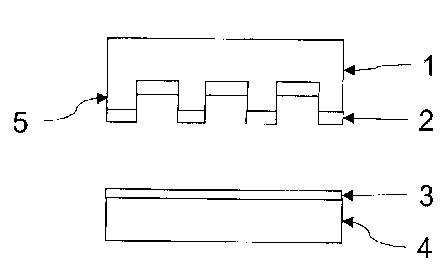
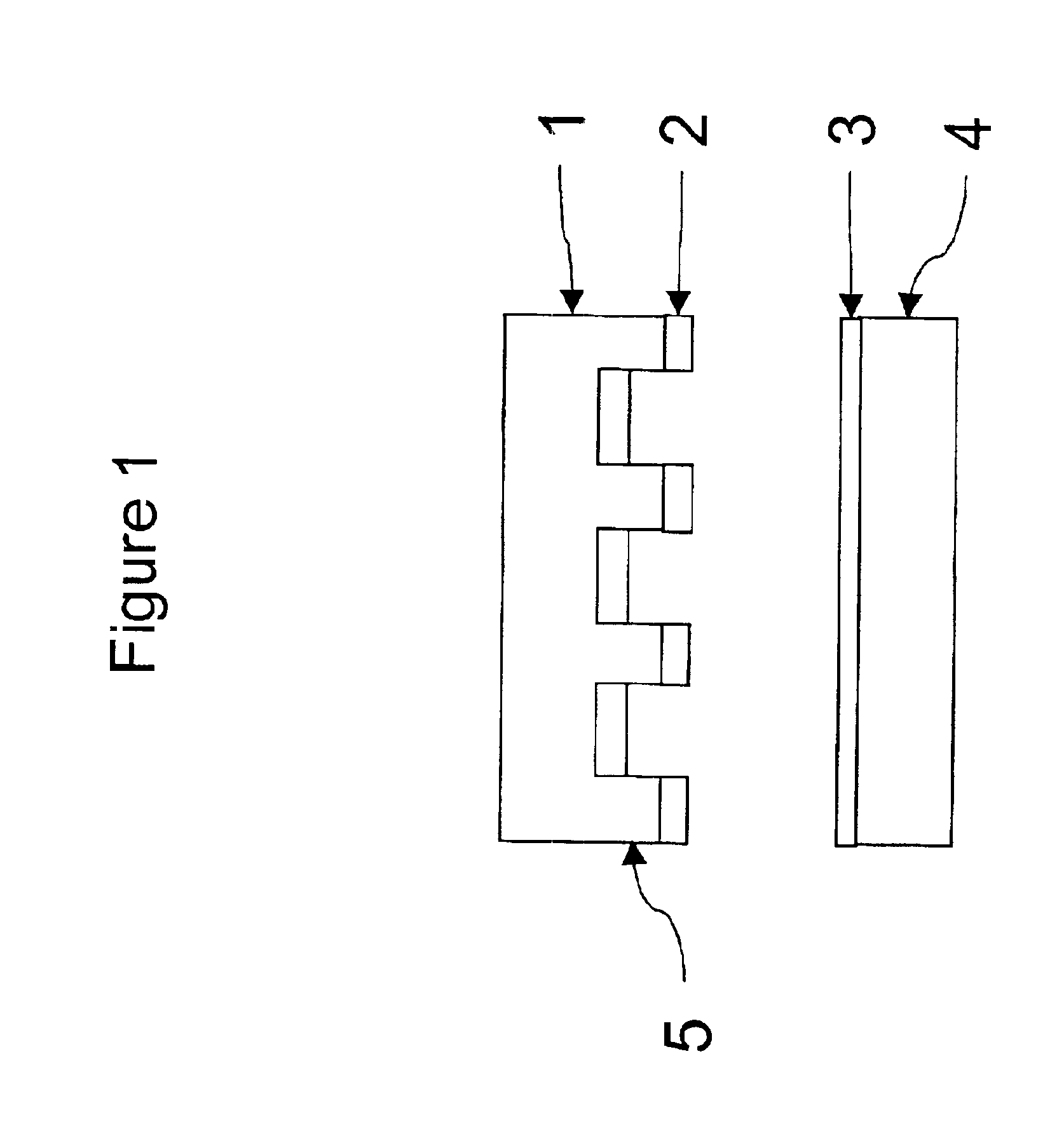
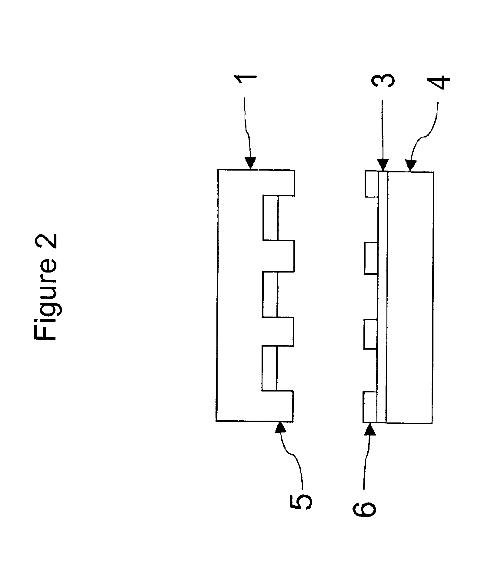
[0086]A method according to the present invention for the direct patterning of metal over a substrate by stamping was performed. Specifically a patterned metal layer was deposited over a substrate by pressing a metal covered die onto an unpatterned thin metal layer with enough pressure so as to cold-weld the metal on the protruding portions of the die to portions of the thin metal film with which the metal formed contact. When the die was removed, the portions of the metal layer cold-welded to the thin metal layer over the substrate detached from the die and remained cold-welded to the thin metal film over the substrate in essentially the same pattern as the die.

[0087]In the present example, a patterning process as shown in FIGS. 6 and 7 was used. A silicon die was patterned using lithography using a phase mask and reactive ion etching. A thin (about 50 Å thick) layer of Alq3 was deposited on the silicon stamp using thermal evaporation. An about 200 Å thick layer of gold was then de...


PUM

PropertyMeasurementUnit
Nanoscale particle sizeaaaaaaaaaa
Thicknessaaaaaaaaaa
Pressureaaaaaaaaaa

Abstract

Methods for patterning a metal over a substrate and devices formed using the methods are disclosed. A patterned die having at least one raised portion and having a metal layer over the die is pressed onto a thin metal film over a substrate, such that the metal layer over the raised portion of the patterned die contacts portions of the thin metal film. Pressure is then applied such that the metal layer and the thin metal film cold-weld to one another. The patterned die is removed, such that the portions of the metal layer cold-welded to the thin metal film break away from the die and remain cold-welded to the thin metal film over the substrate, in substantially the same pattern as the patterned die.

Description

FIELD OF THE INVENTION[0001]The present invention relates to patterning methods for metal, and more particularly to patterning methods using a die. The present invention further relates to devices formed using such methods.BACKGROUND OF THE INVENTION[0002]Nearly all electronic and optical devices require patterning. Patterned metals are used in forming a variety of such devices. For example, patterned metals may be used in forming in transistors, as electrodes in various devices, and as shadow masks in the patterning of various materials.[0003]One possible use for patterned metals is as electrodes in organic light emitting devices (OLEDs), which make use of thin films that emit light when excited by electric current. Popular OLED configurations include double heterostructure, single heterostructure, and single layer, and may be stacked, as described in U.S. Pat. No. 5,707,745, which is incorporated herein by reference in its entirety.[0004]Patterned metals may be achieved by photore...

Claims


Application Information

Patent Timeline
IPC IPC(8): H05K3/10H05K3/20G03F7/00H01L27/32H01L51/52H01L27/28H01L51/40H01L51/50H01L51/05H05K3/04H05K3/02H01L51/00H05K3/38
CPCB82Y10/00B82Y40/00H05K3/108H05K3/20G03F7/0002H01L27/3209H01L51/0021H01L51/5221Y10T29/49155H05K3/386H05K2203/0108H05K2203/095Y10T29/49156H05K3/041H10K59/32H10K71/60H10K50/82
Inventor FORREST, STEPHEN R.KIM, CHANGSOON
Owner THE TRUSTEES FOR PRINCETON UNIV
Why Eureka
Try Eureka