

Method and structure to improve the gate coupling ratio (GCR) for manufacturing a flash memory device
a technology of gate coupling and flash memory, which is applied in the direction of basic electric elements, semiconductor devices, electrical equipment, etc., can solve the problem of only 60% gate coupling ratio, and achieve the effect of improving the gate coupling ratio and increasing the overlapped area
- Summary
- Abstract
- Description
- Claims
- Application Information
AI Technical Summary
Benefits of technology
Problems solved by technology
Method used
Image

Examples
Embodiment Construction
[0025]Reference will be made in detail to the present preferred embodiments of the invention, examples of which are illustrated in the accompanying drawings.
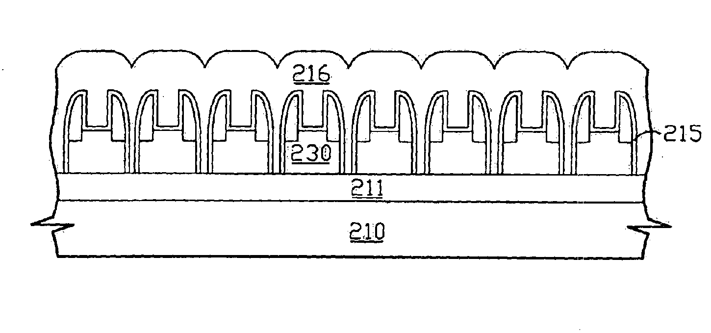
[0026]FIGS. 2A through 2I are schematic cross-sectional views showing the progression of steps for forming a flash memory device according to a preferred embodiment of the current invention. As shown in FIG. 2A, a semiconductor substrate 210, typically a silicon substrate, is provided, and the semiconductor substrate has a plurality of shallow trench isolation (STI) structures (not shown) therein. A gate oxide layer 211 (sometimes called tunnel oxide), a first semiconductor layer 212, typically a polysilicon layer, and an insulating layer 213, typically a silicon nitride layer, are sequentially formed over the semiconductor substrate 210. The first semiconductor layer 212, used as floating gate material, is usually grown by chemical vapor deposition. The insulating layer 213, used as an etching mask for the first semiconductor l...
PUM
 Abstract
Description
Claims
Application Information