Solution for copper hillock induced by thermal strain with buffer zone for strain relaxation

a technology of thermal strain and buffer zone, applied in the direction of basic electric elements, electrical equipment, semiconductor devices, etc., can solve the problems of reducing copper reliability and other defects that cannot be detected accurately, and achieve the effect of reducing copper hillocks and preventing formation of copper hillocks

Active Publication Date: 2005-05-24
TAIWAN SEMICON MFG CO LTD
View PDF9 Cites 8 Cited by
  • Summary
  • Abstract
  • Description
  • Claims
  • Application Information

AI Technical Summary

Benefits of technology

[0010]In accordance with the objects of this invention a new method of reducing copper hillocks in copper metallization is achieved. An opening is made through a dielectric layer overlying a substrate on a wafer. A copper layer is formed overlying the dielectric layer and completely filling the opening. The copper layer is polished back to leave the copper layer only within the opening. Copper hillocks are reduced by applying F ions or a controlled

Problems solved by technology

Copper hillocks reduce copper reliability, cause via induced metal island corrosion (VIMIC

Method used


Image

  • Solution for copper hillock induced by thermal strain with buffer zone for strain relaxation
  • Solution for copper hillock induced by thermal strain with buffer zone for strain relaxation
  • Solution for copper hillock induced by thermal strain with buffer zone for strain relaxation

Examples


Embodiment Construction

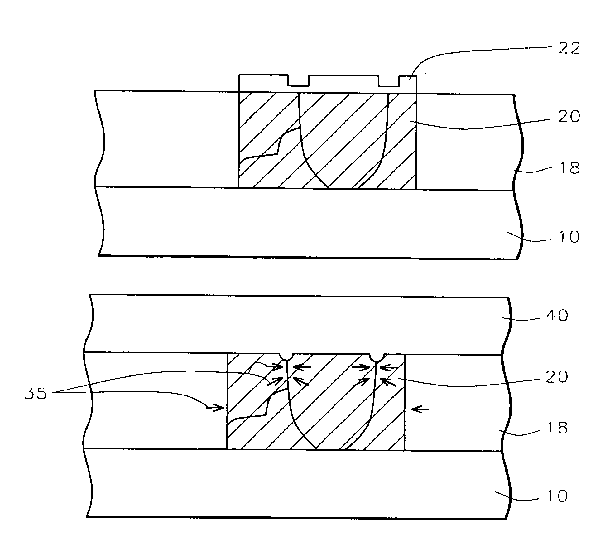
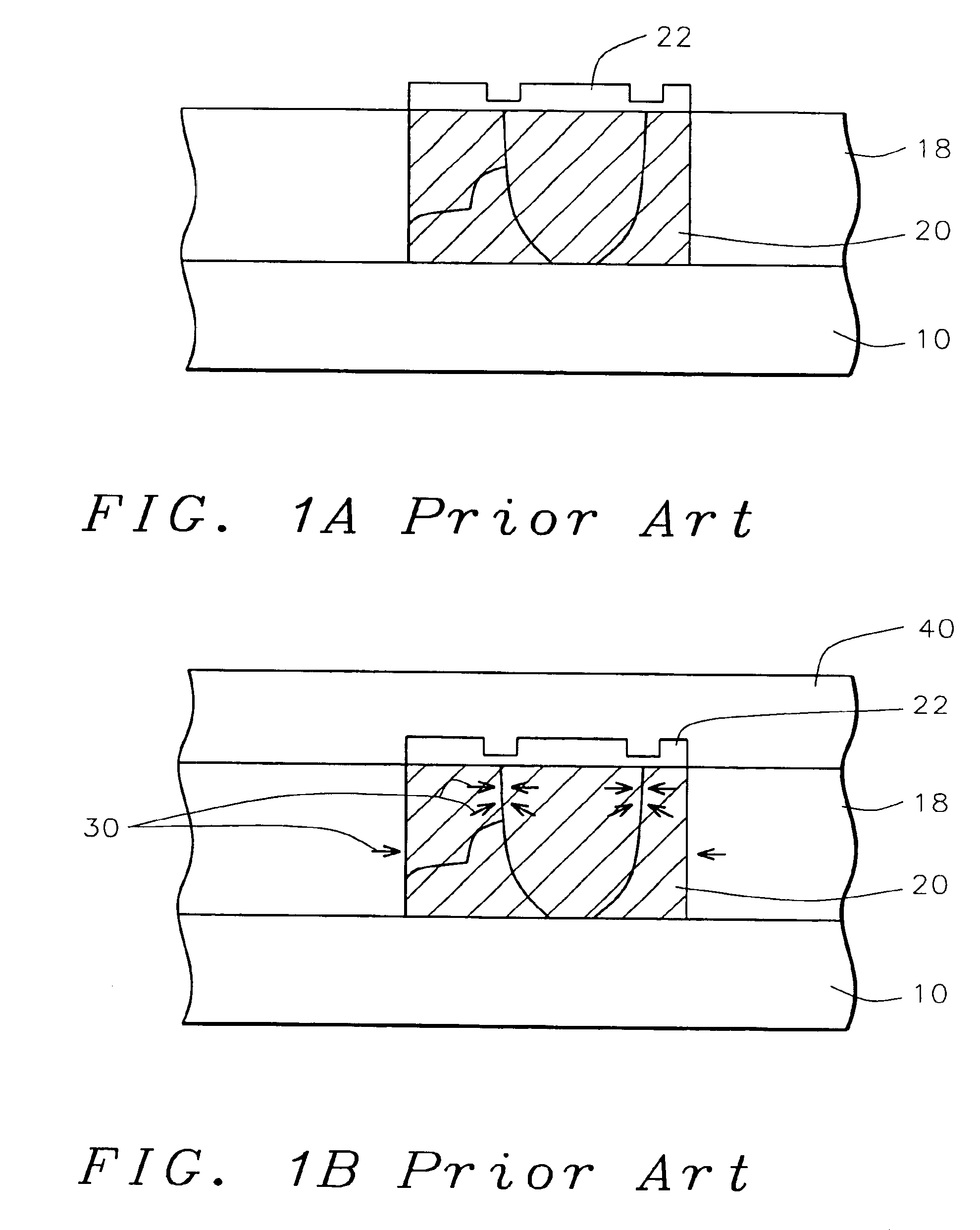
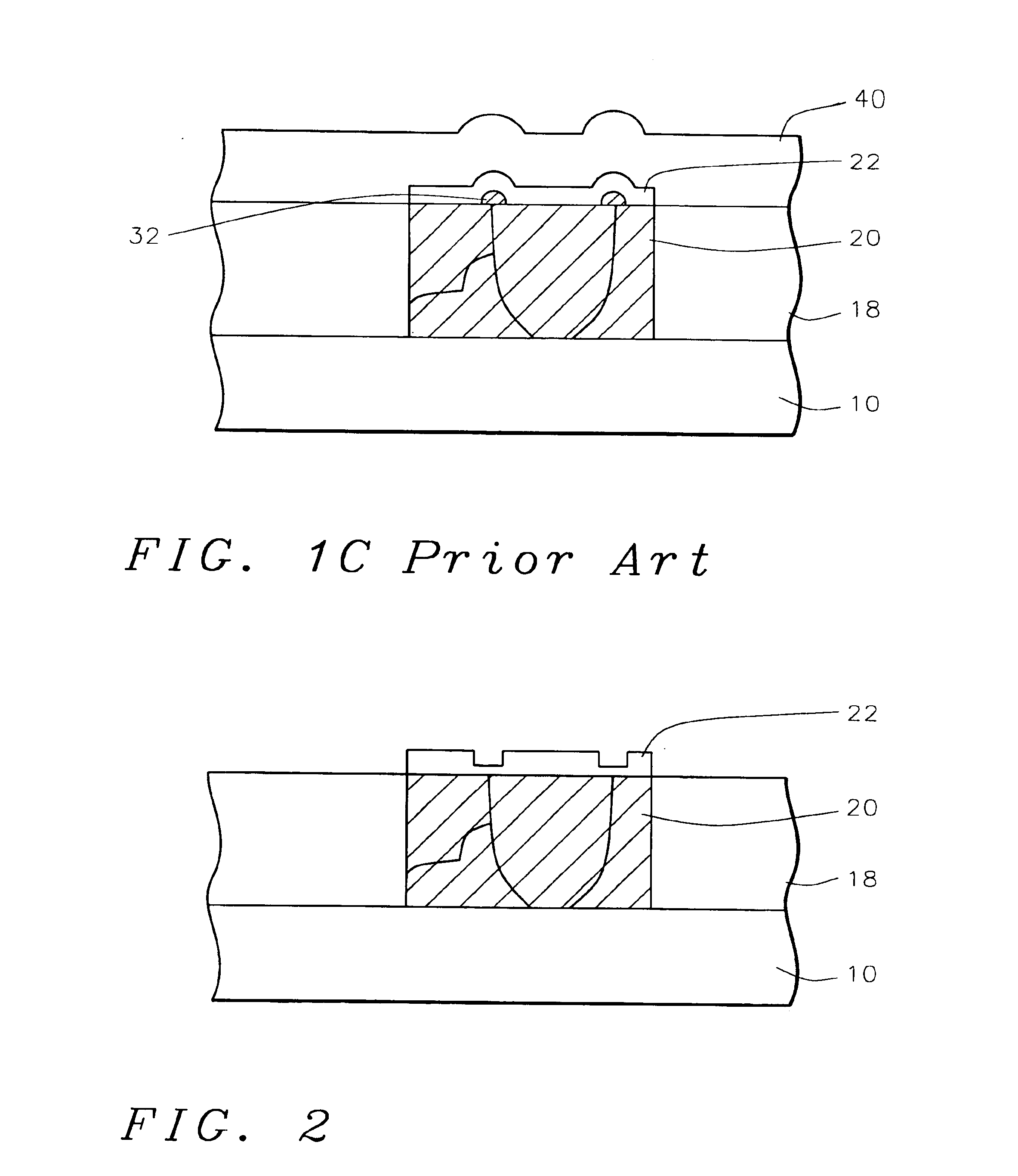
[0015]The present invention provides a method for reducing copper hillocks. Hillocks reduce copper reliability and confuse defect inspection tools. Copper hillock generation after capping layer deposition is caused by compressive-thermal stress on the copper causing a vertical thermal strain on the copper surface.

[0016]Referring now more particularly to FIG. 2, there is illustrated a portion of a partially completed integrated circuit device. There is shown a semiconductor substrate 10, preferably composed of monocrystalline silicon. Semiconductor devices structures may be formed in and on the semiconductor substrate. For example, gate electrodes and source / drain regions as well as lower levels of metallization, not shown, may be formed.

[0017]An insulating layer 18, composed of silicon dioxide, borophosphosilicate glass (BPSG), borosilicate glass (BSG), phosphosilicate glass (PSG), or the like, is deposited over the semiconductor structures to a thickness of between about 6000 and 1...


PUM


Abstract

A method of reducing copper hillocks in copper metallization is described. An opening is made through a dielectric layer overlying a substrate on a wafer. A copper layer is formed overlying the dielectric layer and completely filling the opening. The copper layer is polished back to leave the copper layer only within the opening. Copper hillocks are reduced by applying F ions to the copper layer to form a buffer zone on a surface of the copper layer and in-situ depositing a capping layer overlying the copper layer. The F ions remove copper oxide naturally formed on the copper surface and the buffer zone transfers thermal vertical strain in the copper to horizontal strain thereby preventing formation of copper hillocks.

Description

BACKGROUND OF THE INVENTION[0001](1) Field of the Invention[0002]The invention relates to a method of copper metallization in the fabrication of integrated circuits, and more particularly, to a method of reducing the formation of copper hillocks in copper metallization in the manufacture of integrated circuits.[0003](2) Description of the Prior Art[0004]In a common application for integrated circuit fabrication, a contact / via opening is etched through an insulating layer to an underlying conductive area to which electrical contact is to be made. A conducting layer material is deposited within the contact / via opening. Because of its lower bulk resistivity, Copper (Cu) metallization is the future technology for feature sizes of 0.18 microns and below. Often, a damascene or dual damascene process is used to provide Cu metallization. The copper is deposited within the damascene opening and polished back. Then, a capping layer, such as silicon nitride or silicon carbide, is deposited ove...

Claims


Application Information

Patent Timeline
IPC IPC(8): H01L21/02H01L21/44H01L21/28H01L21/70H01L21/3205H01L21/768
CPCH01L21/76838
Inventor TSAI, SHIN-YEULEU, PO-HSIUNGYANG, CHIA-MINGLIU, TSANG-YUFAN, YUN-DAFAN, CHEN-PENG
Owner TAIWAN SEMICON MFG CO LTD
Why Eureka
Try Eureka