Liquid crystal display device, driving circuit, driving method, and electronic devices

a technology of liquid crystal display and driving circuit, applied in the direction of electric digital data processing, instruments, computing, etc., can solve the problems of power consumption increase and power consumption reduction, and achieve the effects of reducing power consumption, miniaturization and integration, and high-quality screen

Inactive Publication Date: 2005-05-24
BOE TECH GRP CO LTD
View PDF6 Cites 121 Cited by
  • Summary
  • Abstract
  • Description
  • Claims
  • Application Information

AI Technical Summary

Benefits of technology

[0015]In this arrangement, it is preferable for the selector to include: a second switching element inserted between one of said low-level capacitor line and said high-level capacitor line, and the other terminal of said storage capacitor, and the second switching element turns on when the voltage of said selection signal line is one of the high-level and low-level; and a third switching element inserted between the other one of said low-level capacitor line and said high-level capacitor line, and the other terminal of said storage capacitor, and the third switching element turns on when the voltage of said selection signal line is the other one of the high-level and low-level. With this feature, the first, second, and third switching elements can be formed in a common process. Thus, this arrangement is advantageous for reducing power consumption, miniaturization and integration.
[0016]Also, in the arrangement having a selector, it is preferable that the selector have an opposite selection characteristic to the selection characteristic of an adjacent selector in the extending direction of the scanning line. With this feature, the liquid crystal capacitor can be inverted for each data line (column inversion), thereby making it possible to achieve a high-quality screen.
[0017]Further, in the arrangement having a selector, it is most preferable that the selector have an opposite selection characteristic to the selection characteristic of an adjacent selector in the extending direction of the scanning line, and also have an opposite selection characteristic to the selection characteristic of an adjacent selector in the extending direction of the data line. With this feature, the liquid crystal capacitor can be inverted for each pixel, thereby making it possible to achieve high-quality screen.
[0018]Also, the electronic devices according to the present invention are equipped with the above-described liquid crystal display devices, thereby making it possible to reduce power consumption. In this regard, these devices include projectors for extended projection of images, and direct-viewing type displays, for example, display units of personal computers, mobile phones, and any other current or later developed electronic devices that are capable of incorporating the liquid crystal display devices.
[0019]In this regard, the first aspect described above can be accomplished as a driving circuit for a liquid crystal display device. Specifically, a driving circuit for a liquid crystal display device according to a second aspect of the present invention can be provided such that the display device includes: a liquid crystal capacitor arranged at the intersection of a scanning line and a data line, a liquid crystal being sandwiched between a counter electrode and pixel electrode; a first switching element inserted between the data line and the pixel electrode, the first switching element being turned on when the on-voltage is applied to the scanning line, and being turned off when an off-voltage is applied; and a capacitor of which one terminal is connected to the pixel electrode. The driving circuit includes: a scanning line driving circuit which turns the scanning line an on-voltage at every predetermined interval; a data line driving circuit which turns the voltage of the data line to a voltage difference corresponding to a density on the basis of the voltage of the counter electrode and to a writing polarity of the liquid crystal capacitor when the scanning line is on-voltage; and a storage capacitor driving circuit. When the voltage of the data line corresponds to a positive-polarity writing during the period when the scanning line is the on-voltage, the voltage of the other terminal of the storage capacitor is shifted to high after the scanning line turns off, and when the voltage of the data line corresponds to a negative-polarity writing during the period when the scanning line is on-voltage, the voltage of the other terminal is shifted to low after the scanning line turns off. With this arrangement, in the same manner as the first aspect of the present invention, compared with the voltage swing applied to the pixel electrode, the voltage swing of the voltage signal applied to the data line can be maintained to be small, thereby making it possible to reduce power consumption.
[0020]Additionally, the first aspect described above can be accomplished as a driving method for a liquid crystal display device. Specifically, a driving method for a liquid crystal display device according to a third aspect of the present invention can be provided such that the display device includes: a liquid crystal capacitor arranged at the intersection of a scanning line and a data line, a liquid crystal being sandwiched between a counter electrode and pixel electrode; a first switching element inserted between the data line and the pixel electrode, the first switching element being turned on when the on-voltage is-applied to the scanning line, and being turned off when an off-voltage is applied to the scanning line; and a capacitor of which one terminal is connected to the pixel electrode. The driving method includes: turning a scanning line an on-voltage at every predetermined interval; turning a voltage of the data line to a voltage difference corresponding to a density on the basis of the voltage of the counter electrode and to a writing polarity of the liquid crystal capacitor when the scanning line is the on-voltage; and shifting the voltage of the other terminal of the storage capacitor to high after the scanning line turns off when the data line corresponds to a positive-polarity writing during the period when the scanning line is the on-voltage, and shifting the voltage of the other terminal of the storage capacitor to low after the scanning line turns off when the data line corresponds to a negative-polarity writing during the period when the scanning line is the on-voltage. With this arrangement, in the same manner as the first and second aspect of the present invention, compared with the voltage swing finally applied to the pixel electrode, the voltage swing of the voltage signal applied to the data line can be maintained to be small, thereby making it possible to reduce power consumption.

Problems solved by technology

Thus, in an arrangement in which the data line is supplied with a voltage signal having a large swing and with a high frequency, the power consumption increases, which is contrary to lowering the power consumption.

Method used


Image

  • Liquid crystal display device, driving circuit, driving method, and electronic devices
  • Liquid crystal display device, driving circuit, driving method, and electronic devices
  • Liquid crystal display device, driving circuit, driving method, and electronic devices

Examples


first embodiment

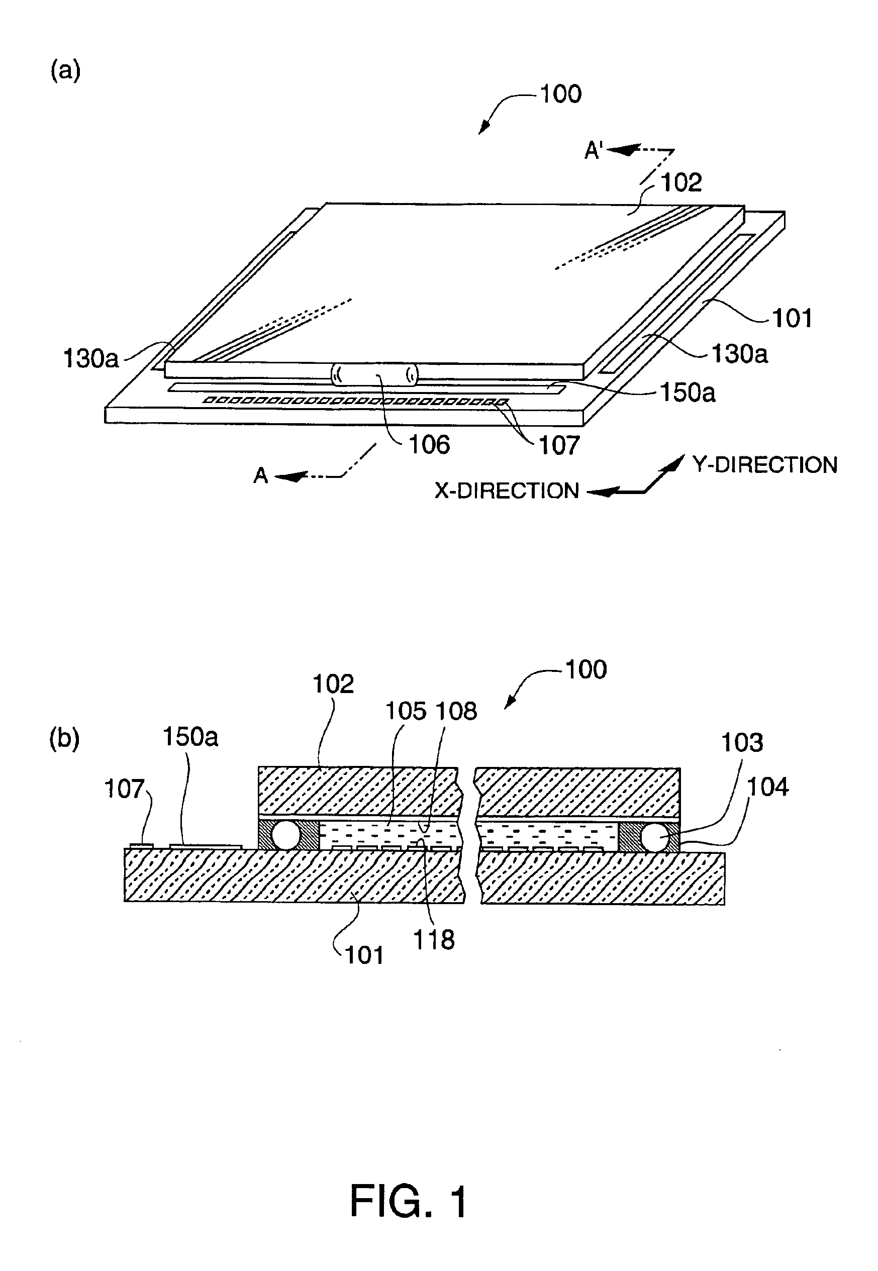
[0038]First, a liquid crystal display device according to a first embodiment of the present invention is described. FIG. 1(a) is a perspective view showing the structure of the liquid crystal display device, and FIG. 1(b) is a cross-sectional view taken along plane A-A′ of FIG. 1(a).

[0039]As shown in FIGS. 1(a) and 1(b), the liquid crystal display device 100 is formed with an element substrate 101 over which various elements and pixel electrodes 118 are arranged, and a counter substrate 102 under which counter electrodes 108 and other elements are arranged. The electrodes are bonded together via a spacer 103 and sealing material 104, while keeping a certain gap between the two with their electrode formed faces facing each other. In the gap, for example, a TN (Twisted Nematic) type liquid crystal 105 is enclosed.

[0040]In this embodiment, the element substrate 101 can be formed of glass, semiconductor, quartz, and any other suitable element, but can also be formed of an opaque substra...

second embodiment

[0126]In the first embodiment as described above, the capacitor line 113 is commonly used for the electrode 120 of each row. Thus, when performing alternating driving of the liquid crystal capacitors, only the inversion per scanning line (row inversion) or inversion per vertical scanning period (frame inversion) can be applied, thereby enabling the remaining factors to increase the power consumption.

[0127]Accordingly, a description will be provided of a second embodiment in which the above shortcoming is enhanced to in some degree. The overall structure of the liquid crystal display device according to the second embodiment is the same as that of the first embodiment as shown in FIG. 1. Thus, the description about this feature is omitted, and the electrical structure will be described.

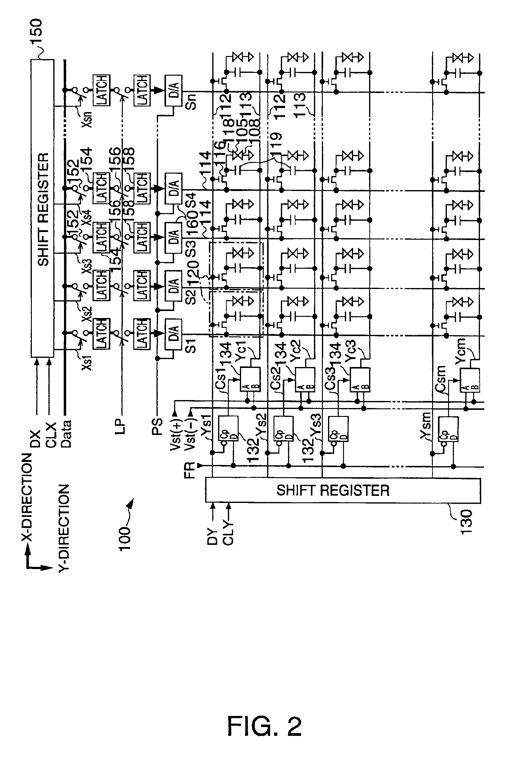
[0128]FIG. 10 is a schematic illustrating the electrical structure of the liquid crystal display device according to the second embodiment of the present invention.

[0129]As shown in FIG. 10, in the sec...

third embodiment

[0137]In the second embodiment, it is true that the power consumption can be reduced as compared to the first embodiment. However, the capacitor lines 113 are divided by the boundary 10. Thus, this will increase the time constant. Consequently, even if the densities of both sides are specified the same, a density difference between the pixels 120 of the both sides of the boundary 10 may occur, thereby deteriorating the display quality.

[0138]Accordingly, a description will be provided of the third embodiment in which enhancements are made for the shortcoming of the deterioration of the display quality. In this regard, since the overall structure of the liquid crystal display device according to the third embodiment is the same as that of the first and the second, the description is omitted. Thus, a description will be provided from the electrical structure.

[0139]FIG. 12 is a schematic illustrating the electrical structure of the liquid crystal display device according to the third em...


PUM

PropertyMeasurementUnit
voltageaaaaaaaaaa
voltageaaaaaaaaaa
voltageaaaaaaaaaa

Abstract

The voltage swing of a data signal, which is supplied to a data line, is maintained to be small, thereby reducing the power consumption. When a scanning signal supplied to a scanning line is set to an on-voltage, a data signal with a voltage, depending on the density and depending on the writing polarity, is applied to a data line. In this case, a TFT is turned on. Thus, a liquid crystal capacitor and storage capacitor store the charge corresponding to the voltage of the data signal. Then, the scanning signal is set to an off-voltage to turn the TFT off, and the voltage of the other terminal of the storage capacitor is raised from the low-level of capacitor voltage to the high-level, and the charge corresponding to the raised voltage amount is redistributed to the liquid crystal capacitor. Thus, the effective voltage value applied to the liquid crystal capacitor can correspond to the voltage swing of the data signal or more.

Description

BACKGROUND OF THE INVENTION[0001]1. Field of Invention[0002]The present invention relates to a liquid crystal display device designed to reduce power consumption, to a driving circuit, to a driving method, and to electronic devices.[0003]2. Description of Related Art[0004]In recent years, liquid crystal display devices (LCD) have been widely used for various information processing devices, flat-screen TVs, and other apparatus as display devices to replace cathode ray tubes (CRT).[0005]These liquid crystal display devices can be classified into various types depending on the driving method and other features. An active-matrix-type LCD device, in which pixels are driven by switching elements, is arranged as follows. Specifically, an active-matrix-type LCD device includes pixel electrodes arranged in a matrix, an element substrate provided with switching elements connected to each of the pixel electrodes, a counter substrate on which counter electrodes are formed to face the pixel elec...

Claims


Application Information

Patent Timeline
Patent Type & Authority Patents(United States)
IPC IPC(8): G09G3/36G02F1/1368G02F1/133G09G3/20
CPCG09G3/3614G09G3/3655G09G3/3688G09G2330/023G09G2310/027G09G2330/021G09G2300/0876G09G3/36
Inventor OZAWA, TOKURO
Owner BOE TECH GRP CO LTD
Why Eureka
Try Eureka