Clock synchronized dynamic memory and clock synchronized integrated circuit
a dynamic memory and clock technology, applied in the field of integrated circuits, can solve the problems of increasing power consumption, power consumption for clock supply, and inability to build a self-refresh function into the dram, and achieve the effect of reducing power consumption
- Summary
- Abstract
- Description
- Claims
- Application Information
AI Technical Summary
Benefits of technology
Problems solved by technology
Method used
Image

Examples
first embodiment
[0052][First Embodiment]
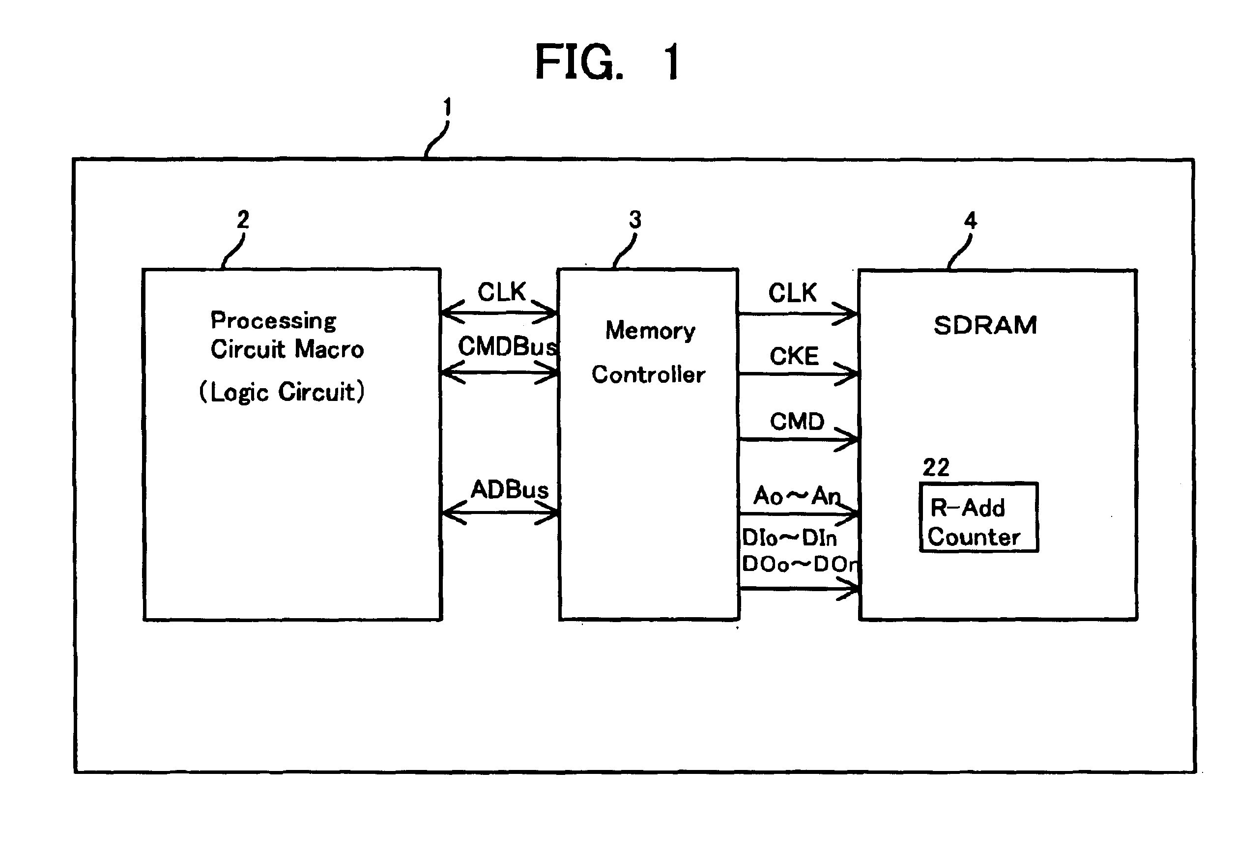
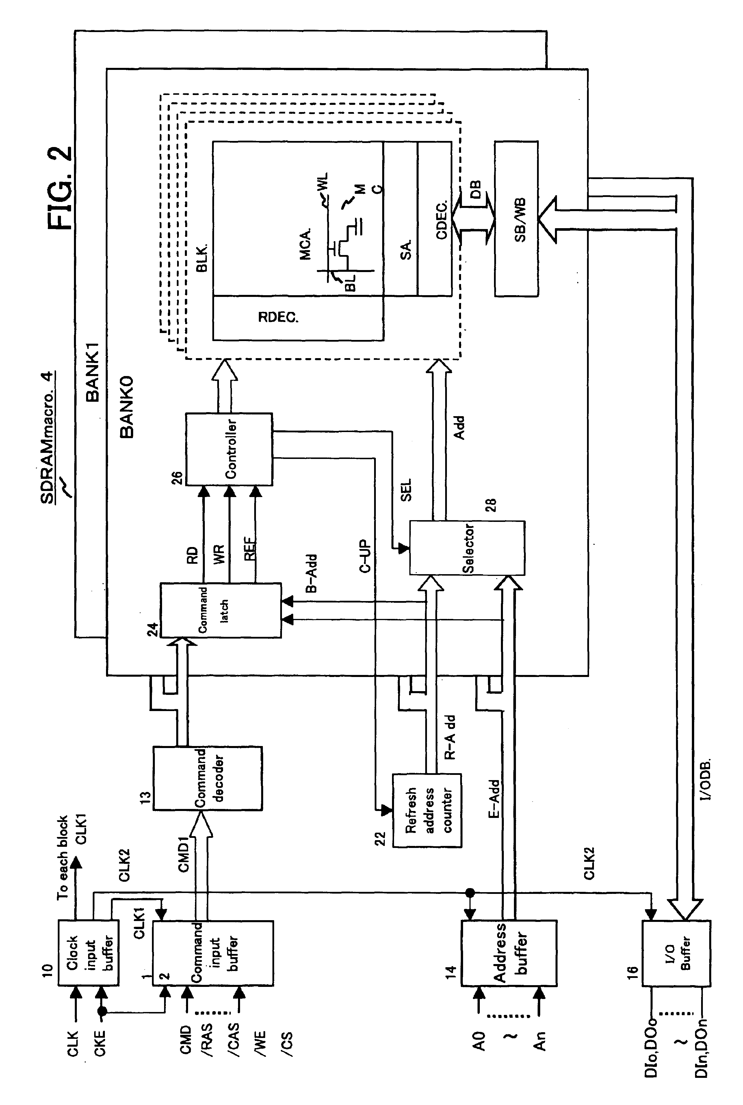
[0053]FIG. 1 is a schematic view of an LSI in which a logic macro and SDRAM macro are embedded in this embodiment. In the embedded LSI 1, there is a processing circuit macro 2 that processes certain data, a synchronous DRAM macro 4, and a memory controller 3 that controls this SDRAM macro. The processing circuit macro 2 has a processor function that processes data corresponding to the use of the embedded LSI. When that data is processed, the SDRAM macro 4 is accessed via the memory controller 3 to store and read large volumes of data. Accordingly, a command bus CMDBus and an address data bus ADBus are provided between the processing circuit macro 2 and the memory controller 3.
[0054]Also, the memory controller 3 reads from and writes to the SDRAM macro 4 in response to an access command from the processing circuit 2. Furthermore, the memory controller 3 also manages the holding of data in the SDRAM macro 4, issues refresh commands in an appropriate cycle, and ...
second embodiment
[0086][Second Embodiment]
[0087]In devices such as DRAM combined logic circuits that fetch data signals in synchronized with a clock signal, to reduce the current consumed during data hold operations, this clock signal need not be distributed to each buffer when there is no change in the data signal being input. Instead it need only be distributed to each buffer when a change in the data signal is detected.
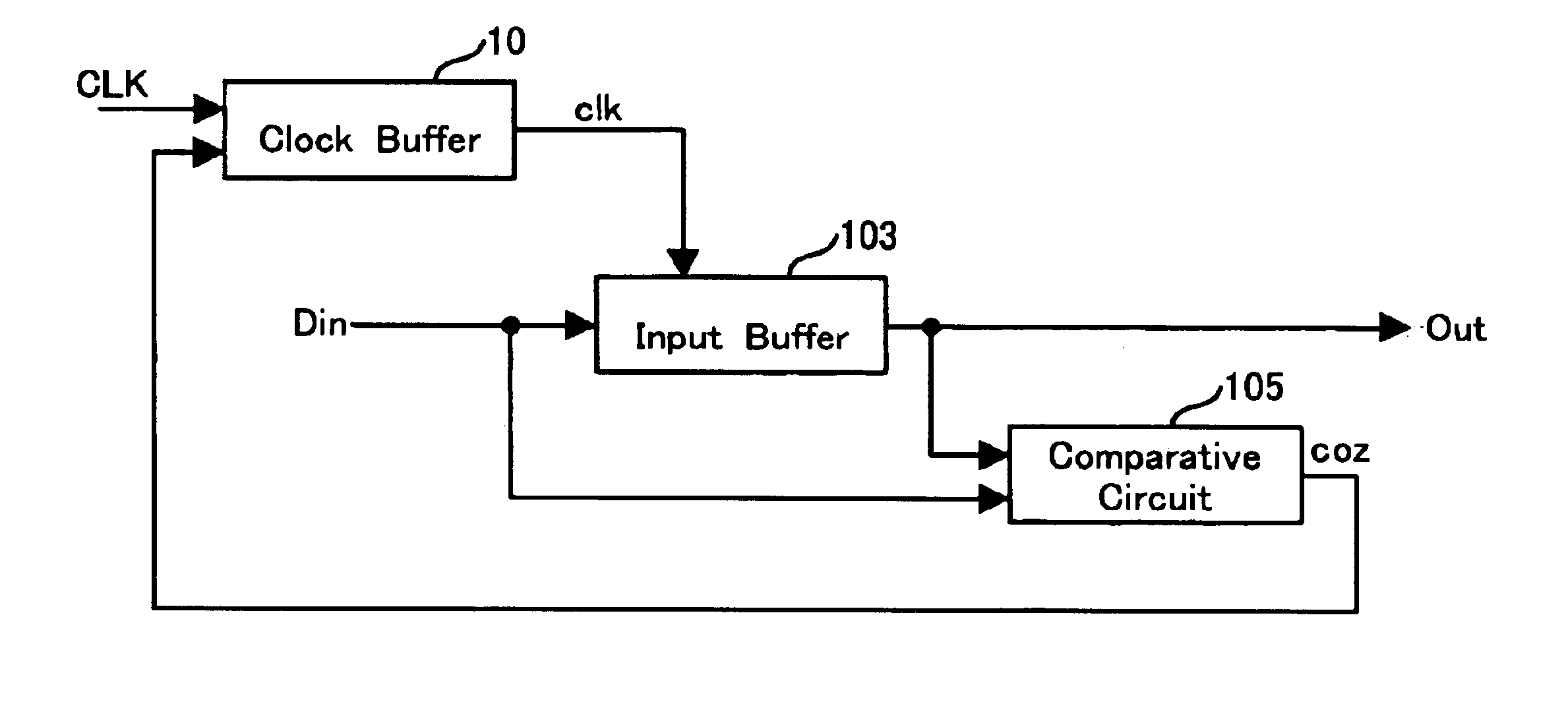
[0088]Below, the integrated semiconductor circuit relating to the second embodiment will be explained. FIG. 10 is a block diagram showing the configuration of a semiconductor integrated circuit relating to this embodiment. As shown in FIG. 10, the integrated semiconductor circuit of this embodiment is equipped with a clock buffer 10, an input buffer 103, and a comparative circuit 105.
[0089]Here, the clock buffer 10 buffers the external clock signal CLK that has been input, generates an internal clock signal clk, then supplies it to the input buffer 103. The input buffer 103 inputs ...
third embodiment
[0105][Third Embodiment]
[0106]In a semiconductor integrated circuit relating to the second embodiment, there is one type of data signal Din that is supplied to the input buffer 103. However, the present invention can also be applied in semiconductor integrated circuits into which a plurality of signal types, including address signals and commands as well as data signals, are input.
[0107]Here, the size of the circuit and the costs involved increase if the clock buffer 10 relating to the above second embodiment is provided for each of this multiplicity of signal types. Therefore, by taking the logical sum of the signals showing that a change in the input signals has been detected, the clock buffers can be combined and thus the number of clock buffers reduced.
[0108]Alternatively, the same clock buffer can be commonly provided for each signal type (function), that is for data, addresses, and commands.
[0109]Below, specific explanation is given of a semiconductor integrated circuit relati...
PUM
 Abstract
Description
Claims
Application Information
 - R&D
- Intellectual Property
- Life Sciences
- Materials
- Tech Scout
- Unparalleled Data Quality
- Higher Quality Content
- 60% Fewer Hallucinations
Browse by: Latest US Patents, China's latest patents, Technical Efficacy Thesaurus, Application Domain, Technology Topic, Popular Technical Reports.
© 2025 PatSnap. All rights reserved.Legal|Privacy policy|Modern Slavery Act Transparency Statement|Sitemap|About US| Contact US: help@patsnap.com