Semiconductor processing apparatus comprising chamber partitioned into reaction and transfer sections

a technology of semiconductor processing equipment and reaction chambers, which is applied in the direction of lighting and heating equipment, charging devices, furniture, etc., can solve the problems of increasing the area occupied by the processing apparatus (the “footprint”) and the width of the front panel of the apparatus (the “faceprint”), reducing and reducing the adhesion of particles. , to achieve the effect of increasing the efficiency of the semiconductor processing equipmen

Inactive Publication Date: 2005-05-31
ASM JAPAN
View PDF103 Cites 397 Cited by
  • Summary
  • Abstract
  • Description
  • Claims
  • Application Information

AI Technical Summary

Benefits of technology

[0016]According to another aspect of the present invention, the reaction chamber is evacuated from a position below the surface of a semiconductor wafer being transferred into the reaction chamber, thereby reducing the adhesion of particles that may be generated when a semiconductor wafer is transferred into the transfer chamber or during deposition. Furthermore, this configuration provides a smaller reaction chamber, thereby increasing the efficiency of the semiconductor processing equipment.

Problems solved by technology

As the number of reaction chambers increases, the area occupied by the processing apparatus (the “footprint”) and the width of the front panel of the apparatus (the “faceprint”) increase, as does the cost of operation.
Additionally, the number of reaction chambers in a layout is limited by the number of sides of the polygon-shaped transfer chamber.
Thus, if the number of reaction chambers is to be increased to improve productivity, the number of gas lines and vacuum pumps must increase as well, thereby increasing the complexity of the processing apparatus.
This configuration allows the footprint or faceprint of the processing apparatus to be reduced to a certain degree, but the reduction is not satisfactory, no improvement of process efficiency or productivity is made, and the total system is generally not simplified.
Furthermore, this configuration makes it difficult to supply wafers to the reaction chambers in a continuous chemical vapor deposition (“CVD”) process, such as in an ashing process.
Finally, during deposition a film is apt to form around the gate valve, thereby necessitating installation of an expensive plasma-proof O-ring for CVD processes using plasma.
Although incorporation of a W-shaped transfer arm into the load lock chamber may solve some of these problems, so doing increases the capacity of the load lock chamber, thereby increasing the time required for evacuating and pressurizing the load lock chamber and thus decreasing processing capacity.

Method used


Image

  • Semiconductor processing apparatus comprising chamber partitioned into reaction and transfer sections
  • Semiconductor processing apparatus comprising chamber partitioned into reaction and transfer sections
  • Semiconductor processing apparatus comprising chamber partitioned into reaction and transfer sections

Examples


Embodiment Construction

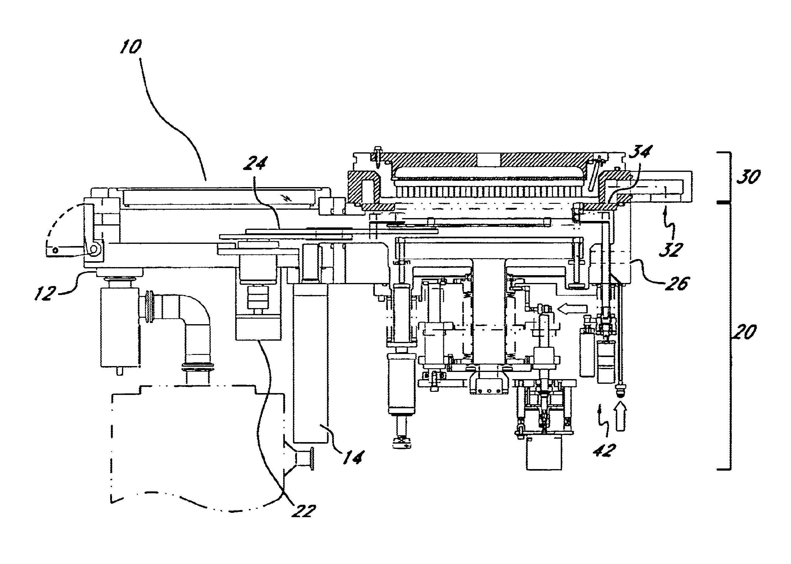
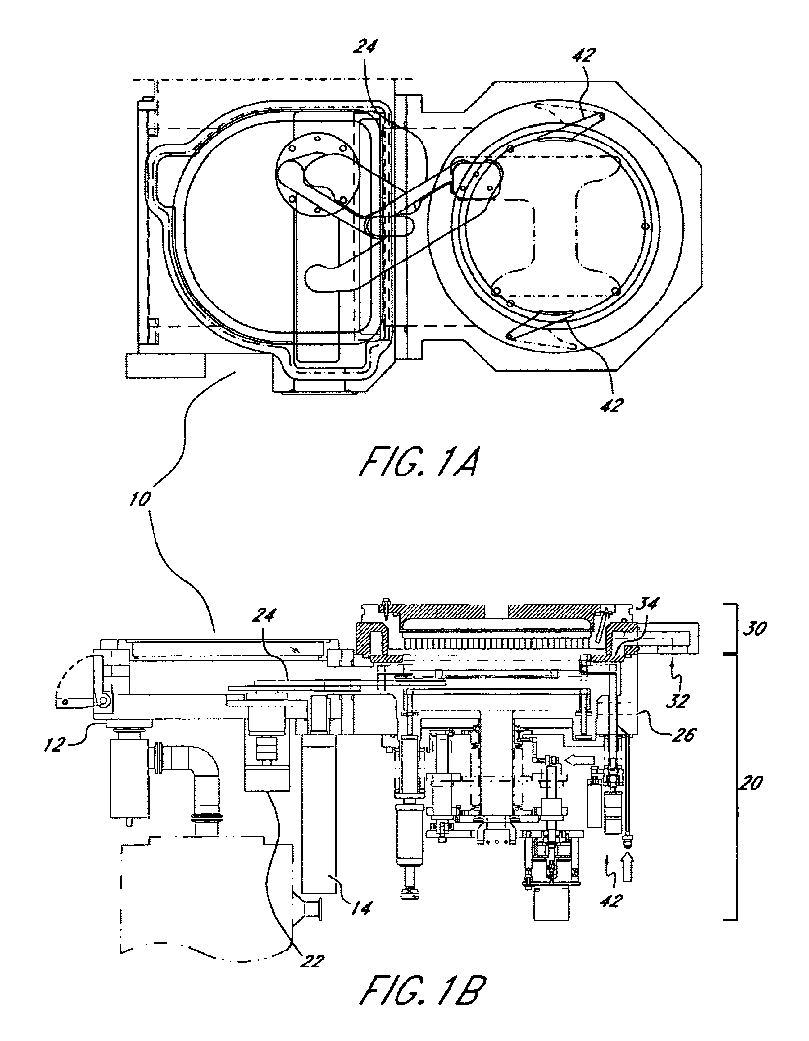
[0023]FIGS. 1 through 4 schematically illustrate one embodiment of semiconductor processing equipment that uses a vacuum load lock system. The embodiment comprises a load lock chamber 10 adapted to queue semiconductor wafers 40 before processing, a transfer chamber 20 and a reaction chamber 30 for growing a film on semiconductor wafers 40. The transfer chamber 20 is positioned adjacent to the load lock chamber 10, and the reaction chamber 30 is positioned above the transfer chamber 20. A transfer robot 22 is positioned outside the load lock chamber 10, and comprises a thin link wafer transfer arm 24 capable of transferring semiconductor wafers 40 from the transfer robot 22 to the load lock chamber 10, the transfer chamber 20, and the reaction chamber 30.

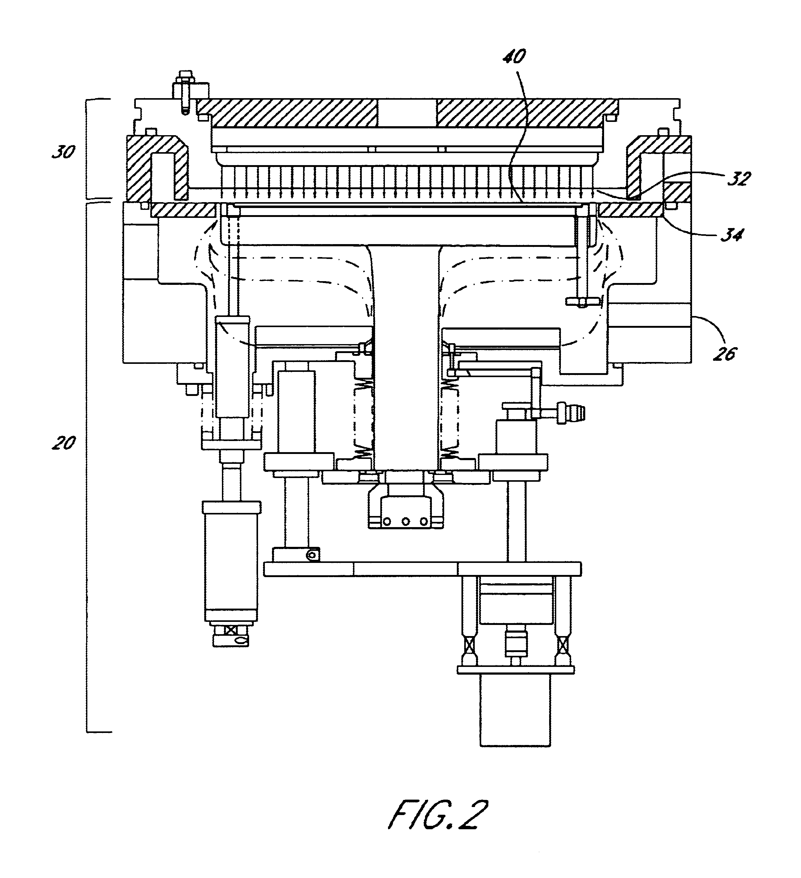
[0024]In such embodiments, the load lock chamber 10 further comprises a load lock exhaust port 12, the transfer chamber 20 further comprises a transfer exhaust port 26, and the reaction chamber 30 further comprises a reaction exhaust...


PUM

PropertyMeasurementUnit
insulatingaaaaaaaaaa
semiconductoraaaaaaaaaa
atmospheric pressureaaaaaaaaaa

Abstract

Semiconductor processing equipment that has increased efficiency, throughput, and stability, as well as reduced operating cost, footprint, and faceprint is provided. Other than during deposition, the atmosphere of both the reaction chamber and the transfer chamber are evacuated using the transfer chamber exhaust port, which is located below the surface of the semiconductor wafer. This configuration prevents particles generated during wafer transfer or during deposition from adhering to the surface of the semiconductor wafer. Additionally, by introducing a purge gas into the transfer chamber during deposition, and by using an insulation separating plate 34, the atmospheres of the transfer and reaction chambers can be effectively isolated from each other, thereby preventing deposition on the walls and components of the transfer chamber. Finally, the configuration described herein permits a wafer buffer mechanism to be used with the semiconductor processing equipment, thereby further increasing throughput and efficiency.

Description

BACKGROUND OF THE INVENTION[0001]1. Field of the Invention[0002]The present invention generally relates to vacuum load lock semiconductor processing equipment, and more specifically relates to compact single-wafer processing semiconductor processing equipment that can efficiently process wafers continuously or simultaneously.[0003]2. Description of the Related Art[0004]Generally, a semiconductor processing apparatus that uses a vacuum load lock system includes a load lock chamber, a transfer chamber and multiple reaction chambers that are connected to the transfer chamber. For each apparatus, a substrate-handling robot is used to automatically supply substrates to the reaction chambers. In such an arrangement, an atmospheric robot first brings a substrate inside the load lock chamber from a cassette or a front opening unified pod (“FOUP”). The FOUP may comprise a detachable cassette and a box with a front-opening interface. After the substrates are placed in the load lock chamber, t...

Claims


Application Information

Patent Timeline
Patent Type & Authority Patents(United States)
IPC IPC(8): H01L21/677H01L21/67C23C16/44B65G49/07
CPCH01L21/67742H01L21/67748Y10S414/139H01L21/02
Inventor YAMAGISHI, TAKAYUKISUWADA, MASAEIWATANABE, TAKESHI
Owner ASM JAPAN
Why Eureka
Try Eureka