Stochastic assembly of sublithographic nanoscale interfaces

a nano-scale interface and nano-scale technology, applied in nanoinformatics, instruments, semiconductor/solid-state device details, etc., can solve the problem of complicated discovery of connected wires, and achieve the effect of reasonable efficiency and tighter address encoding

Inactive Publication Date: 2005-05-31
CALIFORNIA INST OF TECH +3
View PDF18 Cites 83 Cited by
  • Summary
  • Abstract
  • Description
  • Claims
  • Application Information

AI Technical Summary

Benefits of technology

[0035]The address decoder can be assembled without relying on lithographic patterning at nanoscale dimensions by randomly mixing differently coded nanoscale wires and enabling them to self-assemble into a parallel array at right angles to a pre-existing array of microwires. The approach according to the present disclosure realizes a microscale-to-nanoscale interface, bridging the gap from top-down lithographic processing to bottom-up self-assembly. The differently-coded nanoscale wire-based address decoder according to the present disclosur...

Problems solved by technology

Additionally, the approach relies on strongly quantized connection values for each intersection, while imprecisely localized gold nanoparticles could lead to i...

Method used


Image

  • Stochastic assembly of sublithographic nanoscale interfaces
  • Stochastic assembly of sublithographic nanoscale interfaces
  • Stochastic assembly of sublithographic nanoscale interfaces

Examples


first embodiment

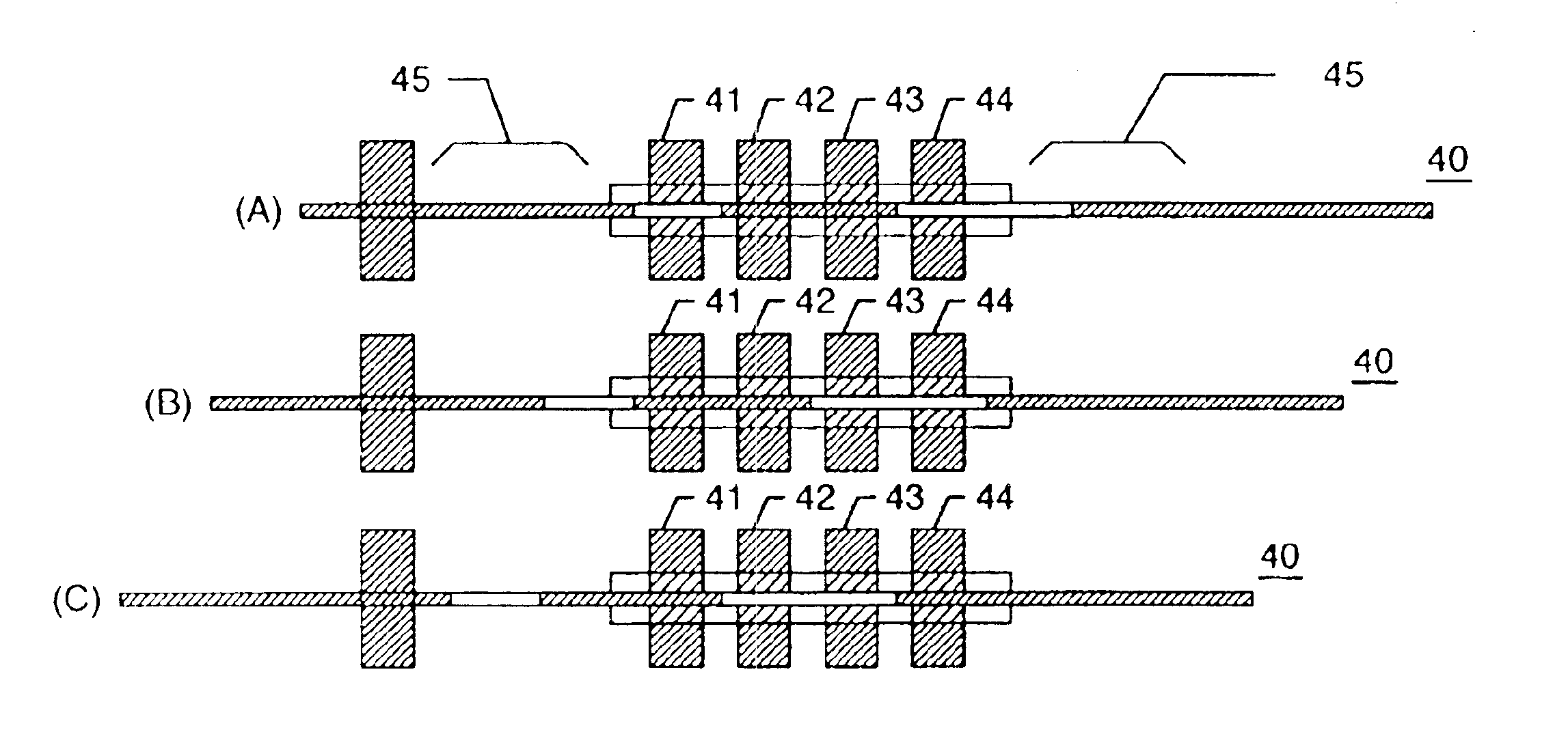
[0106]FIG. 14 shows a first embodiment for controlling staggered ohmic contacts, where four microscale wires 701-704 and an interface logic 705 are provided. Microscale wire 702 controls whether the operation is a write operation or a read operation, thus allowing communication either to the ohmic contacts or from the ohmic contacts. If the operation is a read operation, the signal is read on the output wire 701. The contacts 110-112 are selected by means of the wires 703, 704. Usually, N contacts will require log2N selection wires.

second embodiment

[0107]FIG. 15 shows a second embodiment for controlling staggered ohmic contacts, in case compact access to the decoder is more important than high-speed access. In this embodiment, only microscale wires 801-804 are needed. Microscale wire 801 carries the shift signal, microscale wire 802 carries the clock signal, microscale wire 803 carries the shift input signal, and microscale wire 804 carries the shift output signals. With a higher number of contacts, more time and a higher number of flip-flops are required, but not a higher number of microscale wires.

[0108]Also in the hybrid control case, control wires can either be microscale wires (as shown) or nanoscale wires.

One-dimensional Memory

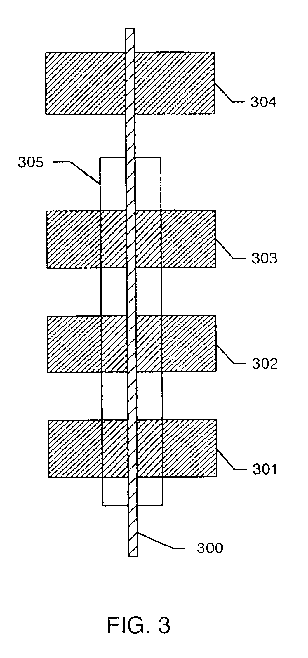
[0109]The embodiment of FIG. 11 shows a two-dimensional memory. The present disclosure also provides a one-dimensional memory embodiment, using a single nanowire layer, as shown in FIG. 16.

[0110]FIG. 16 is similar to FIG. 13, and shows staggered microscale wire contacts 110-112 energizing the endpo...


PUM


Abstract

A method for controlling electric conduction on nanoscale wires is disclosed. The nanoscale wires are provided with controllable regions axially and/or radially distributed. Controlling those regions by means of microscale wires or additional nanoscale wires allows or prevents electric conduction on the controlled nanoscale wires. The controllable regions are of two different types. For example, a first type of controllable region can exhibit a different doping from a second type of controllable region. The method allows one or more of a set of nanoscale wires, packed at sublithographic pitch, to be independently selected.

Description

CROSS REFERENCE TO RELATED APPLICATIONS[0001]This application claims the benefit of U.S. provisional Patent Application Ser. No. 60 / 398,943 filed Jul. 25, 2002 for a “Modulation Doped Molecular-Scale Address Decoding” by André DeHon, Patrick Lincoln, U.S. provisional Patent Application Ser. No. 60 / 400,394 filed Aug. 1, 2002 for a “Implementation of Computation Note 15: Integration Issues for Modulation Doped Memory” by André DeHon, Patrick Lincoln, U.S. provisional Patent Application Ser. No. 60 / 415,176 filed Sep. 30, 2002 for “Nanoscale Architectures based on Modulation Doping” by André DeHon, Patrick Lincoln, Charles Lieber, U.S. provisional Patent Application Ser. No. 60 / 429,010 filed Nov. 25, 2002 for “Stochastic Assembly of Sublithographic Nanoscale Interfaces” by André DeHon, Patrick Lincoln, John E. Savage, U.S. provisional Patent Application Ser. No. 60 / 441,995 filed Jan. 23, 2003 for “Stochastic Assembly of Sublithographic Nanoscale Interfaces” by Andre' DeHon, Charles Lieb...

Claims


Application Information

Patent Timeline
IPC IPC(8): G11C13/02H01L23/52H01L23/522H01L29/06H01L29/02H01L27/10G11C13/00G11C8/10H01L21/3205H01L49/00
CPCB82Y10/00G11C8/10G11C13/0023G11C13/02G11C13/025H01L23/522H01L27/101H01L29/0665H01L29/0673H01L49/00H01L2924/0002G11C2213/71G11C2213/77G11C2213/81Y10S977/762Y10S977/943H01L2924/00H10N99/00
Inventor DEHON, ANDRELIEBER, CHARLES M.LINCOLN, PATRICK D.SAVAGE, JOHN E.
Owner CALIFORNIA INST OF TECH
Why Eureka
Try Eureka