Diffused extrinsic base and method for fabrication

a technology of extrinsic base and fabrication method, which is applied in the direction of transistors, semiconductor devices, electrical equipment, etc., can solve the problems of affecting the reducing the frequency performance of the base resistor, so as to improve the high speed performance, reduce the base resistence, and improve the transistor performance. effect of performan

Inactive Publication Date: 2005-05-31
GLOBALFOUNDRIES US INC
View PDF15 Cites 94 Cited by
  • Summary
  • Abstract
  • Description
  • Claims
  • Application Information

AI Technical Summary

Benefits of technology

[0008]Accordingly, the present invention provides a unique device structure and method that provides increased transistor performance in integrated bipolar circuit devices. The preferred embodiment of the present invention provides improved high speed performance by providing reduced base resistence. The preferred design forms the extrinsic base by diffusing dopants from a dopant source layer into the extrinsic base region. This diffusion of dopants forms at least a portion of the extrinsic base. In particular, the portion adjacent to the intrinsic base region is formed by diffusion. This solution avoids the problems caused by traditional solutions that implanted the extrinsic base. Specifically, by forming at least a portion of the extrinsic base by diffusion, the problem of damage to base region is minimized. Additionally, the formed extrinsic base can have improved resistence, resulting in an improved maximum frequency for the bipolar device. Additionally, the extrinsic base can be formed with a self-aligned manufacturing process that reduces fabrication complexity and thus lower cost.

Problems solved by technology

Unfortunately, most methods to reduce base resistence are hampered by: 1) implantation enhanced diffusion of the intrinsic base dopant caused by the implantation process for the extrinsic base which widens the intrinsic base and thus reduces its frequency performance; 2) high wafer cost caused by a complex transistor process; and 3) difficulty of integrating the NPN device process with the CMOS process steps.
Without an improved method and structure for forming such devices the performance of these devices will continue to be compromised.

Method used


Image

  • Diffused extrinsic base and method for fabrication
  • Diffused extrinsic base and method for fabrication
  • Diffused extrinsic base and method for fabrication

Examples


Embodiment Construction

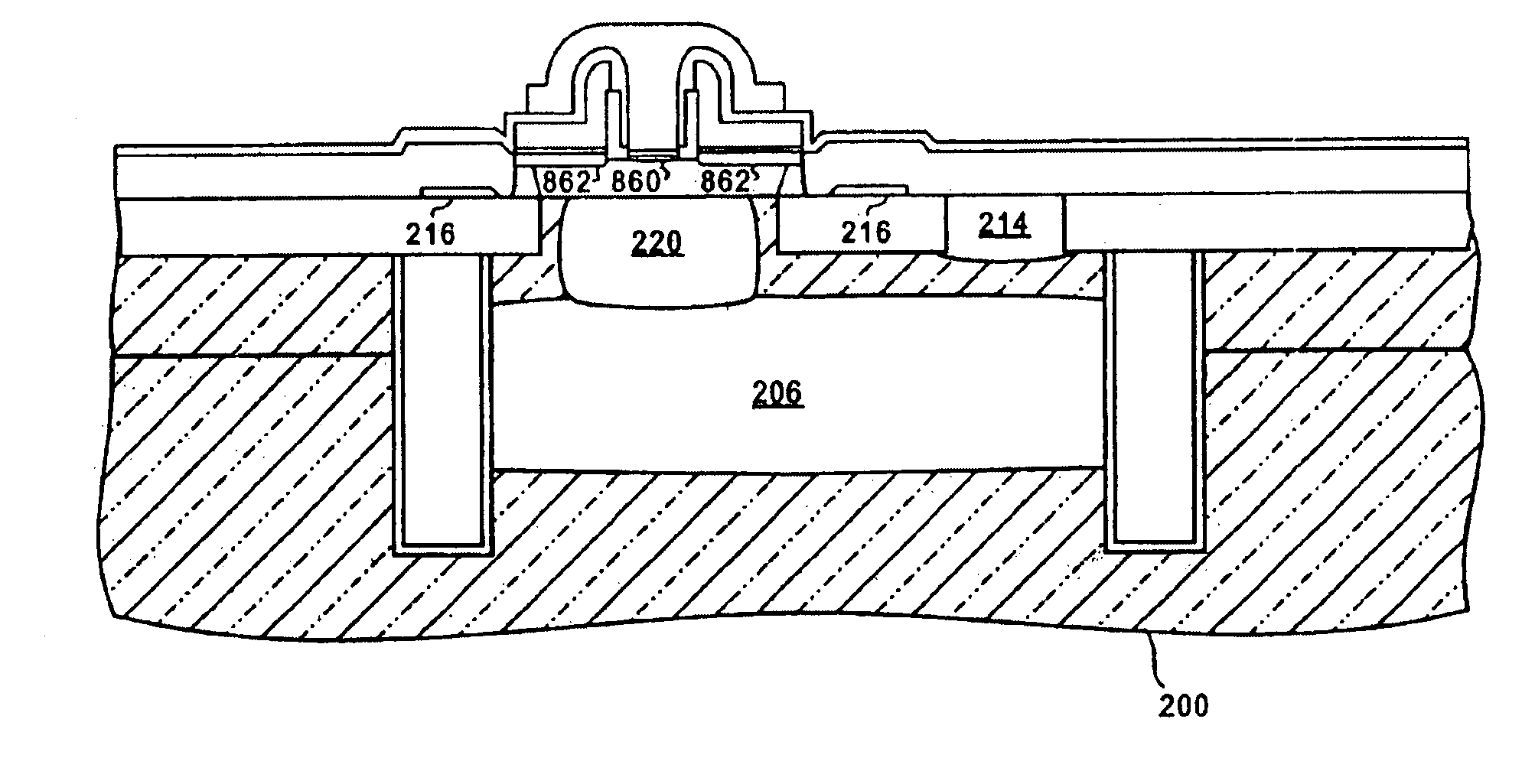
[0015]The present invention provides a unique device structure and method that provides increased transistor performance in integrated bipolar circuit devices. The preferred embodiment of the present invention provides improved high speed performance by providing reduced base resistence. The preferred design forms the extrinsic base by diffusing dopants from a dopant source layer and into the extrinsic base region. This diffusion of dopants forms at least a portion of the extrinsic base. In particular, the portion adjacent to the intrinsic base region is formed by diffusion. This solution avoids the problems caused by traditional solutions that implanted the extrinsic base. Specifically, by forming at least a portion of the extrinsic base by diffusion, the problem of damage to base region is minimized. This reduced damage enhances dopant diffusion into the intrinsic base. Additionally, the formed extrinsic base can have improved resistence, resulting in an improved maximum frequency...


PUM


Abstract

The present invention provides a unique device structure and method that provides increased transistor performance in integrated bipolar circuit devices. The preferred embodiment of the present invention provides improved high speed performance by providing reduced base resistence. The preferred design forms the extrinsic base by diffusing dopants from a dopant source layer and into the extrinsic base region. This diffusion of dopants forms at least a portion of the extrinsic base. In particular, the portion adjacent to the intrinsic base region is formed by diffusion. This solution avoids the problems caused by traditional solutions that implanted the extrinsic base. Specifically, by forming at least a portion of the extrinsic base by diffusion, the problem of damage to base region is minimized. This reduced damage enhances dopant diffusion into the intrinsic base. Additionally, the formed extrinsic base can have improved resistence, resulting in an improved maximum frequency for the bipolar device. Additionally, the extrinsic base can be formed with a self-aligned manufacturing process that reduces fabrication complexity.

Description

[0001]This application is a divisional of Ser. No. 10 / 064,476; filed on Jul. 18, 2002.BACKGROUND OF THE INVENTION[0002]1. Technical Field[0003]The present invention relates generally to the field of semiconductor manufacturing and, more specifically, to a method for forming improved transistors that have improved high frequency response.[0004]2. Background Art[0005]The need to remain cost and performance competitive in the production of semiconductor devices has caused continually increasing device performance requirements in integrated circuits. To facilitate the increase in circuit functionality, new technologies are constantly needed to increase the performance of the semiconductor devices. This improvement in device performance may involve higher frequency performance as well as increased frequency performance at low current densities which enables low power circuit designs. However, a successful technology must provide high performance with increased circuit performance at low ...

Claims


Application Information

Patent Timeline
Patent Type & Authority Patents(United States)
IPC IPC(8): H01L21/331H01L21/02H01L21/70H01L29/10H01L21/8249H01L29/02
CPCH01L21/8249H01L29/66287H01L29/1004
Inventor CANTELL, MARC W.DUNN, JAMES S.HARAME, DAVID L.JOHNSON, ROBB A.LANZEROTTI, LOUIS D.ST. ONGE, STEPHEN A.TESSIER, BRIAN L.WUTHRICH, RYAN W.
Owner GLOBALFOUNDRIES US INC
Why Eureka
Try Eureka