Massively parallel atomic layer deposition/chemical vapor deposition system

Inactive Publication Date: 2005-06-07
EUGENUS INC
View PDF19 Cites 83 Cited by
  • Summary
  • Abstract
  • Description
  • Claims
  • Application Information

AI Technical Summary

Benefits of technology

[0019]The vertically stacked ALD/CVD reactors have a low height profile, but allow separate gas inlet at the top of a chamber and separate exhaust at the bottom of the chamber to provide a generally axi-symmetric vertical gas flow across the wafer when the wafer is processed in the reactor chambers. The vertical arrangement allows multiple wafers to be processed separately in module housing the multiple reactors.
[0020]In one embodiment, the reactor chamber is formed by placing a top plate and a bottom plate onto a frame. The top plate and the bottom may have a particularly shaped recessed regions

Problems solved by technology

In reference to ALD processes, batch ALD reactors are believed to be difficult to maintain relative to single wafer reactors, which historically have had the capability for in-situ clean

Method used


Image

  • Massively parallel atomic layer deposition/chemical vapor deposition system
  • Massively parallel atomic layer deposition/chemical vapor deposition system
  • Massively parallel atomic layer deposition/chemical vapor deposition system

Examples


Example

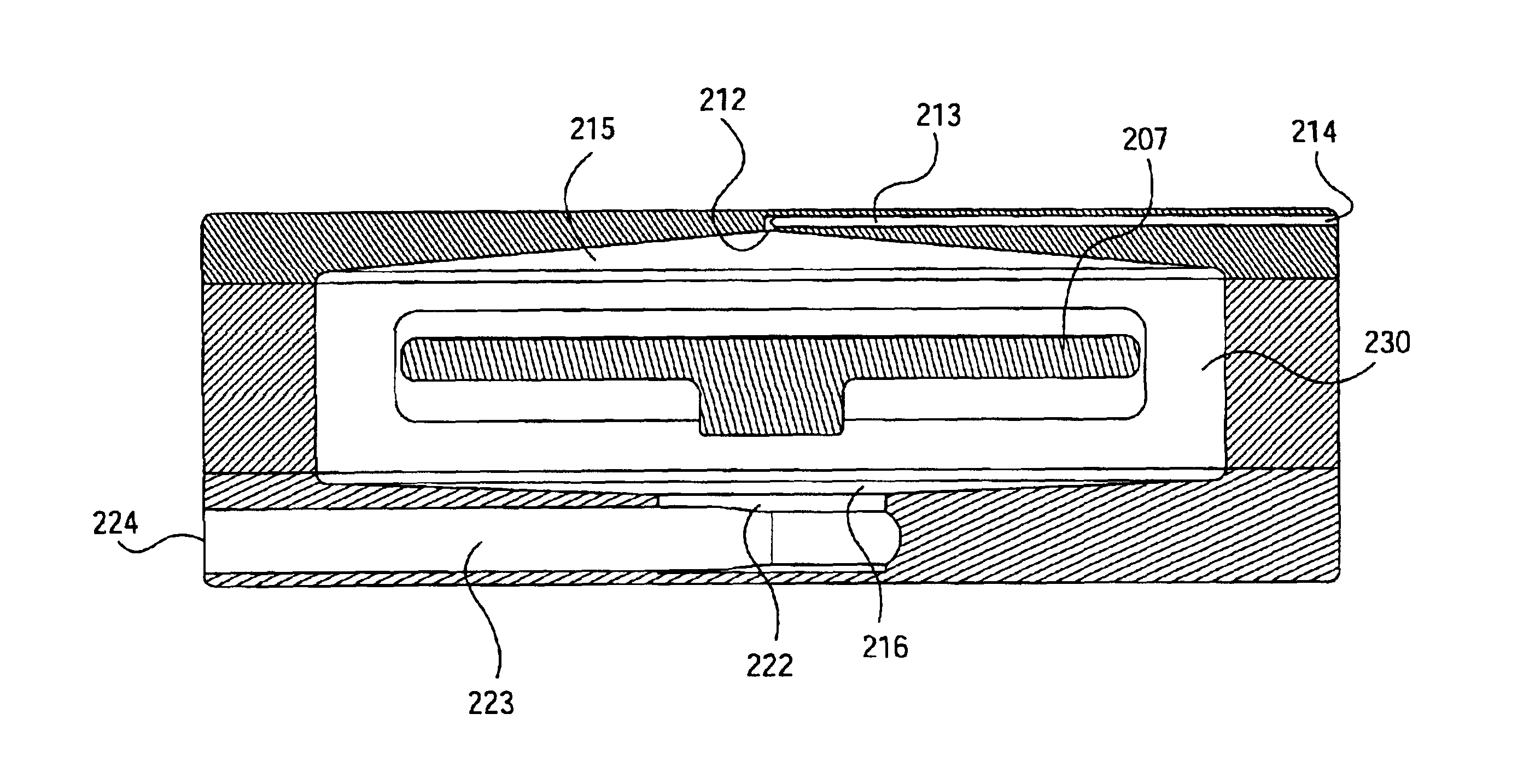
[0021]In the description below, the present invention is described in reference to various embodiments. The example embodiments are described in terms of depositing film material on a substrate by Atomic Layer Deposition (ALD). Although ALD is described, the method and apparatus may be readily adapted for the practice of Chemical Vapor Deposition (CVD) or variants thereof. However, the practice of the invention is not limited to these processes. Furthermore, the substrate may be of a variety of base materials for depositing subsequent material layers and need not be limited to the deposition of film layers on a semiconductor substrate (wafer). For example, substrates used for manufacture of flat panel displays may readily be the base substrate.

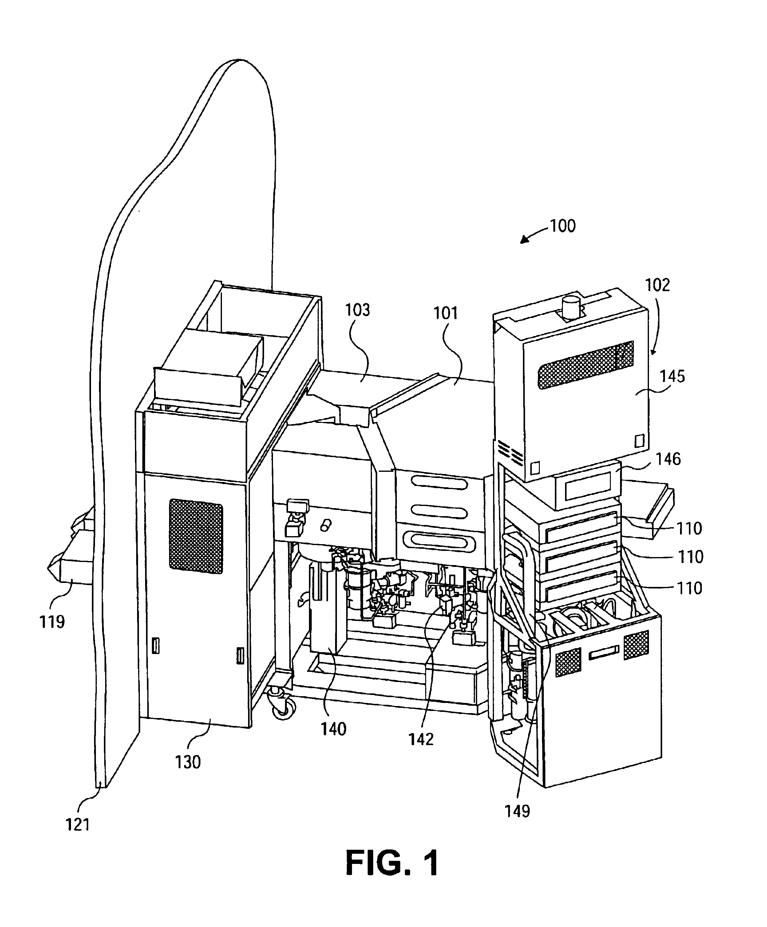
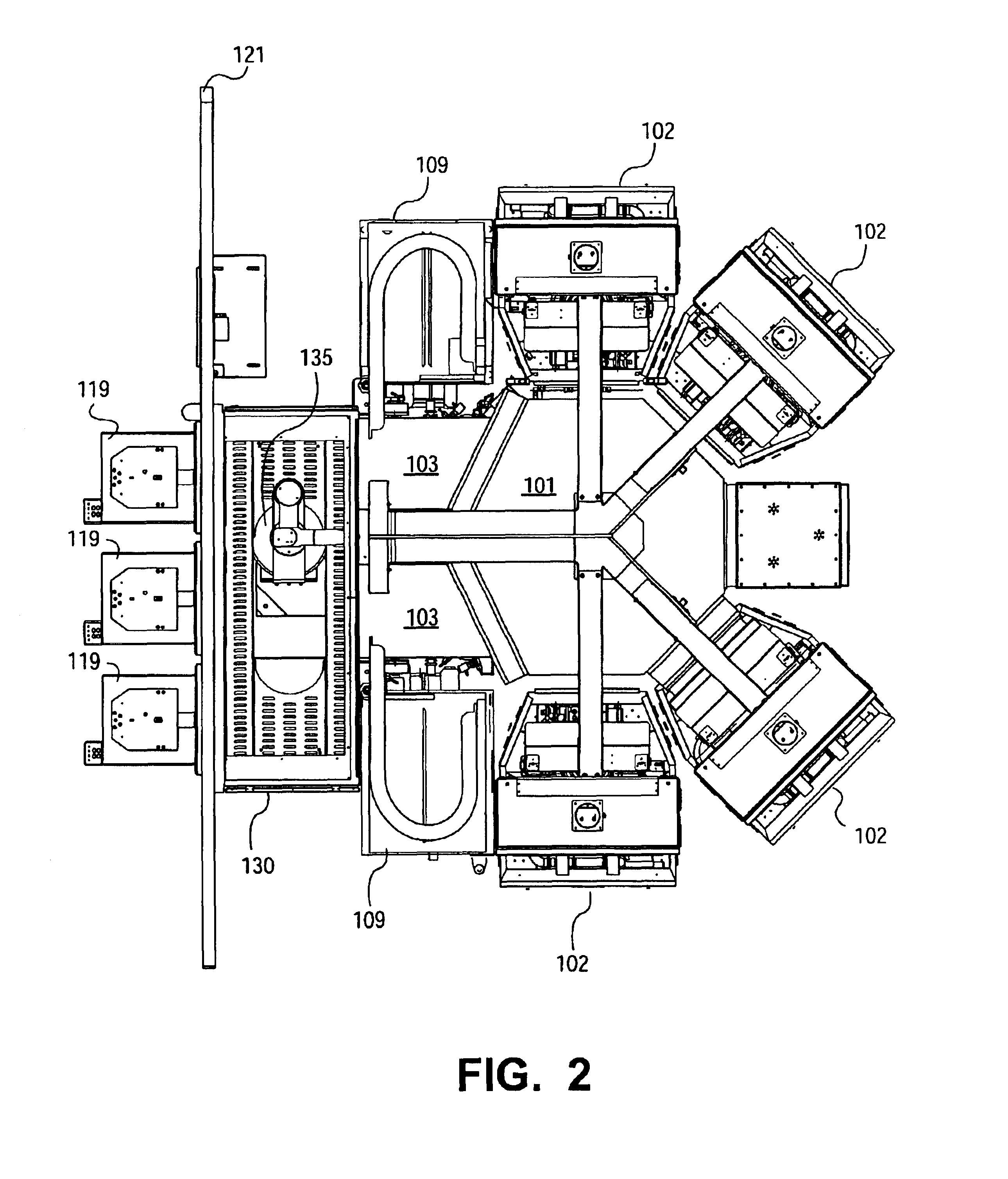
[0022]Referring to FIG. 1, an example embodiment of a Massively Parallel ALD System (MPAS) 100 is shown. A top plan view and a side plan view of the MPAS 100 are respectively shown in FIGS. 2 and 3 (in FIG. 3, only one process module is shown)...


PUM

PropertyMeasurementUnit
Lengthaaaaaaaaaa
Flow rateaaaaaaaaaa
Shapeaaaaaaaaaa

Abstract

A method and apparatus for the use of individual vertically stacked ALD or CVD reactors. Individual reactors are independently operable and maintainable. The gas inlet and output are vertically configured with respect to the reactor chamber for generally axi-symmetric process control. The chamber design is modular in which cover and base plates forming the reactor have improved flow design.

Description

CROSS-REFERENCE TO RELATED APPLICATION[0001]This application claims the benefit of priority from U.S. Provisional Patent Application Ser. No. 60 / 346,005 entitled “Massively Parallel ALD / CVD System” filed on Oct. 29, 2001.FIELD OF THE INVENTION[0002]The present invention relates to semiconductor processing and, more particularly, to an apparatus and method for providing a massively parallel ALD / CVD system.BACKGROUND OF THE RELATED ART[0003]Chemical Vapor Deposition (CVD) is a widely used deposition process for the growth of thin films on various substrates, including semiconductor wafers. As microelectronics device dimensions are reduced, or scaled down, CVD is an attractive method for the deposition of conformal films over complex device topography. In the field of atomic / molecular level film deposition, a process known as Atomic Layer Deposition (ALD) has emerged as a promising candidate to extend the abilities of CVD techniques. Generally, ALD is a process wherein conventional CVD...

Claims


Application Information

Patent Timeline
IPC IPC(8): C23C16/54C23C16/44C23C16/455
CPCC23C16/4412C23C16/54C23C16/45546C23C16/45544
Inventor SEIDEL, THOMAS E.JANSZ, ADRIANPUCHACZ, JUREKDOERING, KEN
Owner EUGENUS INC
Why Eureka
Try Eureka