
Semiconductor device

a semiconductor device and semiconductor technology, applied in the field of vertical, can solve the problems of increasing on-loss, affecting the stability of the device, so as to improve the breakdown voltage, prevent the device from being broken down, and prevent the effect of being broken down

Inactive Publication Date: 2005-06-07
FUJI ELECTRIC SYST CO LTD
View PDF8 Cites 59 Cited by
  • Summary
  • Abstract
  • Description
  • Claims
  • Application Information

AI Technical Summary

Benefits of technology

[0020]The breakdown voltage of the semiconductor device according to the invention is high, since depletion layers expand in the OFF-state of the semiconductor device from very many pn-junctions not only to the drain drift region but also to the portion of the semiconductor chip outside the drain drift region and the deep portion of the semiconductor chip near the second major surface due to the provision of the second alternating conductivity type layer with a second repeating pitch which is narrower than a first repeating pitch in the breakdown withstanding region. Since the curved electric line of force extending from the side of the active region to the layer with low electrical resistance via the breakdown withstanding region is longer than the electric line of force extending from the active region on the side of the first major surface to the layer with low electrical resistance via the drain drift region, the electric field strength in the breakdown withstanding region is lower than that in the drain drift region even when the impurity concentrations in both regions are the same. Therefore, the breakdown voltage in the breakdown withstanding region is higher than that in the drain drift region. Since a high breakdown voltage is obtained in the breakdown withstanding region of the super-junction semiconductor device including a drain drift region formed of an alternating conductivity type layer, the structure of the alternating conductivity type layer in the drain drift region is optimized easily, a super-junction MOSFET is designed more freely, and the resulting MOSFET is a practical one.
[0036]Advantageously, the outermost second semiconductor region of the first alternating conductivity type layer in contact with the innermost third semiconductor region of the second alternating conductivity type layer is connected to the second well region of the second conductivity type. Since the pn-junction between the second semiconductor region of the second conductivity type of the first alternating conductivity type layer and the third semiconductor region of the first conductivity type of the second alternating conductivity type layer is connected to the second well region of the second conductivity type, dynamic avalanche breakdown is hardly caused. Moreover, this structure facilitates adjusting the charge balance between the second semiconductor region and the fifth semiconductor region in contact with each other.

Problems solved by technology

Therefore, breakdown is caused at a voltage lower than the designed breakdown voltage of the semiconductor device.
However, a thick n-type drift layer 12 inevitably causes high on-resistance, which further causes on-loss increase.
However, the provision of the alternating conductivity type layer makes it more difficult to obtain a higher breakdown voltage in the breakdown withstanding region by adding the conventional depletion electric field control means including the guard ring and the field plate.
Therefore, the provision of the alternating conductivity type layer makes it more difficult to optimally design the additional means for correcting the depletion electric field strength in the breakdown withstanding region, and impairs the reliability of the semiconductor device.
Thus, it has been impossible to fully realize the functions expectable to the super-junction semiconductor devices.
However, when dynamic avalanche breakdown is caused below the gate pad or below the field plate, the excessive carriers are accumulated once on the boundary between the gate pad and the insulation film, and are then discharged at once toward the portion of the source electrode layer surrounding the gate pad, causing breakdown of the semiconductor device due to the generated heat and such causes.
Therefore, the withstanding capability against dynamic avalanche breakdown is inevitably lower in the portions of the semiconductor chip below the gate pad than in the drain drift region, causing an unstable breakdown voltage.

Method used


Image

  • Semiconductor device
  • Semiconductor device
  • Semiconductor device

Examples


first embodiment

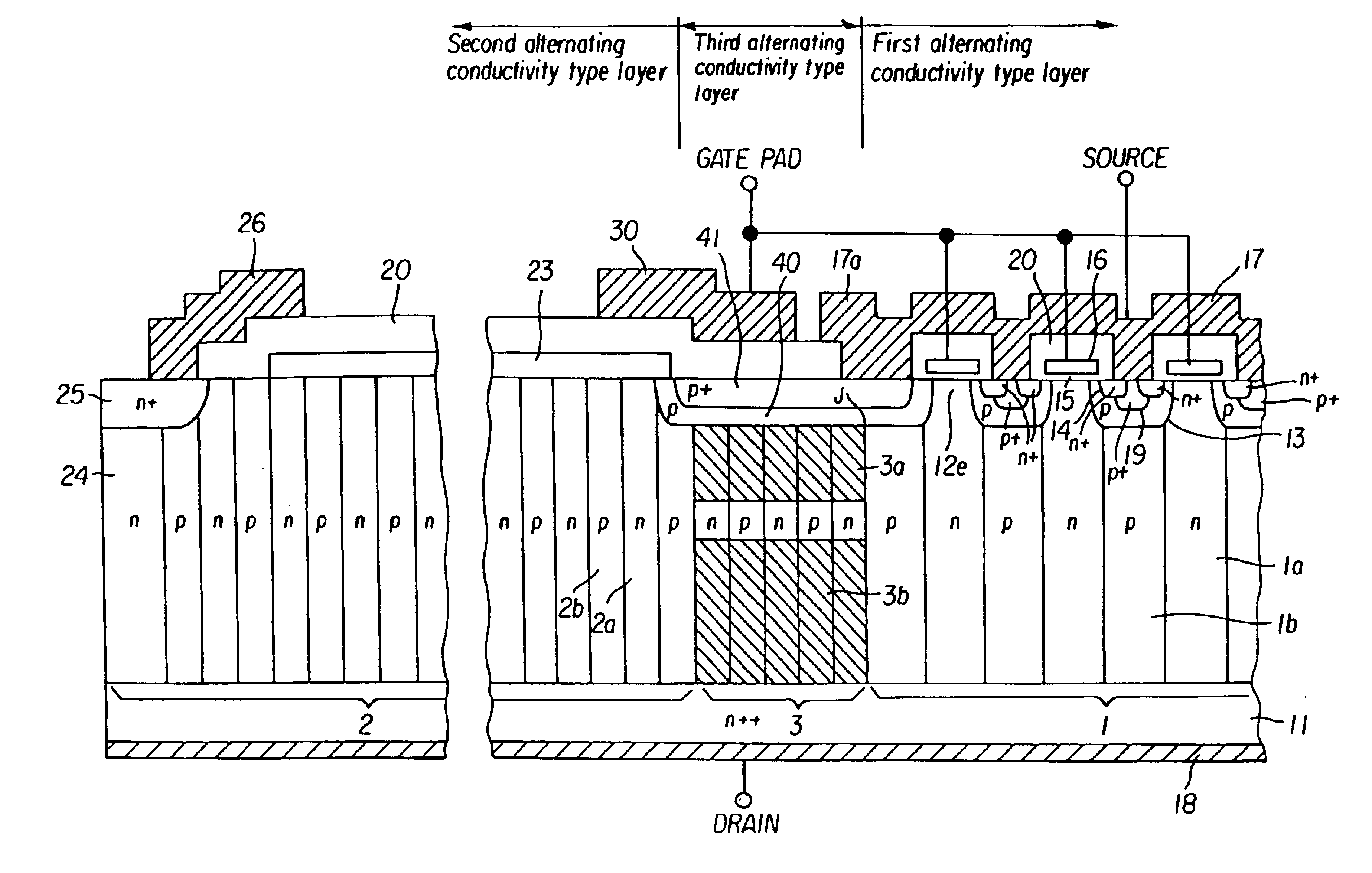
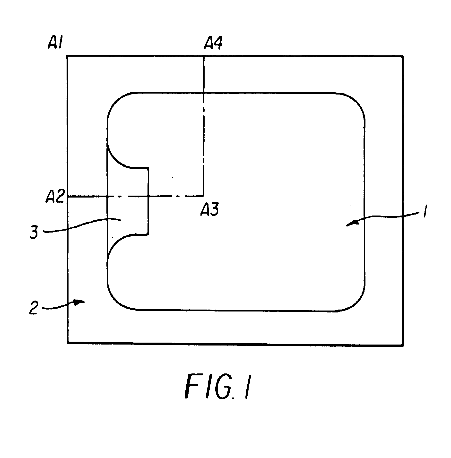
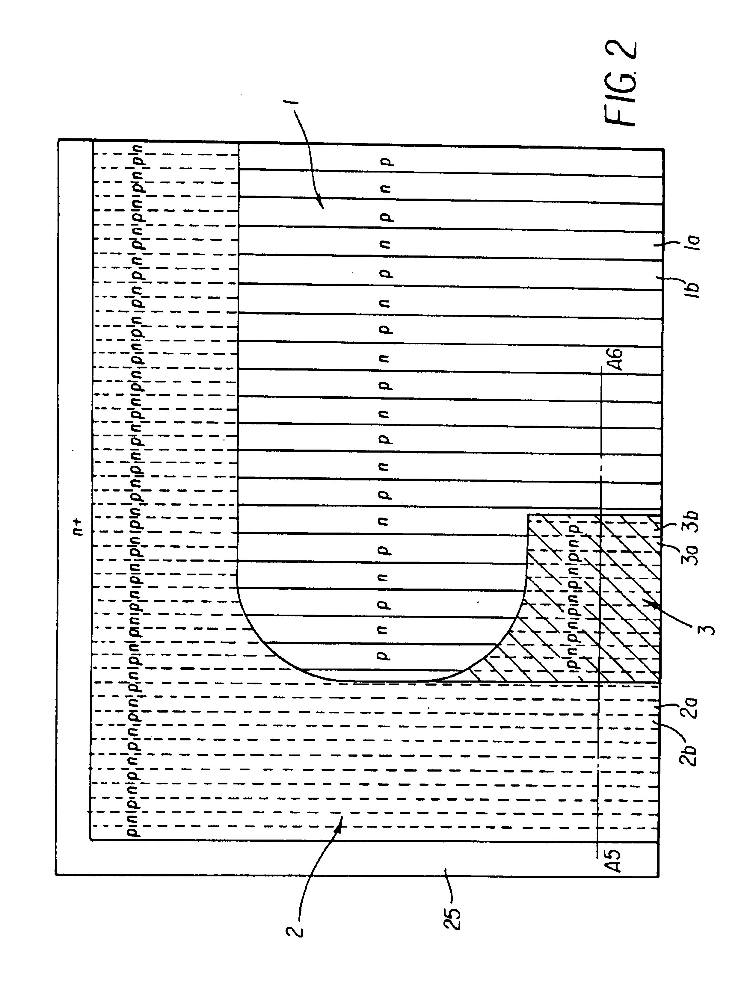
[0053]FIG. 1 is a top plan view of the semiconductor chip of a vertical MOSFET according to a first embodiment of the invention. The surface active region, the source electrode layer and the gate pad on the insulation film are omitted from FIG. 1. FIG. 2 is an expanded top plan view of the rectangular area defined by the lines A1-A2-A3-A4 of FIG. 1. FIG. 3 is a cross section along A5-A6 of FIG. 2.

[0054]The vertical MOSFET according to the first embodiment includes a drain electrode 18 on the back surface of a semiconductor chip; an n++-type drain layer (drain contact layer) 11 with low electrical resistance in electrical contact with drain electrode 18; a drain drift region 1 including a first alternating conductivity type layer on n++-type drain layer 11; heavily doped p-type base regions 13 in the surface portion of drain drift region 1, p-type base regions 13 being cells selectively formed and shaped with respective rings or stripes; a heavily doped n+-type source region 14 forme...

second embodiment

[0072]FIG. 5 is an expanded top plan view showing the upper left area of a vertical MOSFET according to a second embodiment of the invention. The area shown in FIG. 5 corresponds to the rectangular area as shown in FIG. 2 and as defined by the lines A1-A2-A3-A4 in FIG. 1.

[0073]The MOSFET according to the second embodiment includes a drain drift region 1 including a first alternating conductivity type layer, a breakdown withstanding region 2 including a second alternating conductivity type layer and an under region 3 including a third alternating conductivity type layer. The MOSFET according to the second embodiment is different from the MOSFET according to the first embodiment in that the boundaries between the n-type regions and the p-type regions in the second and third alternating conductivity type layers are extending in perpendicular to the boundaries between the n-type drift regions and p-type partition regions in the first alternating conductivity type layer. The n-type drift...

third embodiment

[0075]FIG. 6 is a top plan view of the semiconductor chip of a vertical MOSFET according to a third embodiment of the invention. The surface active region, the source electrode layer and the gate pad on the insulation film are omitted from FIG. 6. FIG. 7 is an expanded top plan view of the rectangular area defined by the lines B1-B2-B3-B4 of FIG. 6. The cross section along B5-B6 of FIG. 7 is the same with FIG. 3.

[0076]The MOSFET according to the third embodiment includes a drain drift region 1 including a first alternating conductivity type layer, a breakdown withstanding region 2 including a second alternating conductivity type layer, and an under region 3 including a third alternating conductivity type layer below a gate pad. Under region 3 is positioned at a corner of drain drift region 1. The pn-junctions in drain drift region 1 and the pn-junctions in under region 3 are extending in parallel to each other laterally. The pn-junctions in drain drift region 1 and the pn-junctions ...


PUM


Abstract

A semiconductor device facilitates obtaining a higher breakdown voltage in the portion of the semiconductor chip around the drain drift region and improving the avalanche withstanding capability thereof. A vertical MOSFET according to the invention includes a drain layer; a drain drift region on drain layer, drain drift region including a first alternating conductivity type layer; a breakdown withstanding region (the peripheral region of the semiconductor chip) on drain layer and around drain drift region, breakdown withstanding region providing substantially no current path in the ON-state of the MOSFET, breakdown withstanding region being depleted in the OFF-state of the MOSFET, breakdown withstanding region including a second alternating conductivity type layer, and an under region below a gate pad, and the under region including a third alternating conductivity type layer.

Description

[0001]This application is a Division of Ser. No. 10 / 073,671 Feb. 11, 2002 U.S. Pat. No. 6,674,126.FIELD OF THE INVENTION[0002]The present invention relates to vertical power semiconductor devices such as MOSFET's (insulated gate field effect transistors), IGBT's (insulated gate bipolar transistors), bipolar transistors and diodes. Specifically, the present invention relates to vertical power semiconductor devices which facilitate realizing a high breakdown voltage and a high current capacity.BACKGROUND[0003]Semiconductor devices may be classified into lateral devices, which arrange the main electrodes thereof on one major surface and make a drift current flow in parallel to the major surface, and vertical devices, which distribute the main electrodes thereof on two major surfaces facing opposite to each other and makes a drift current flow in perpendicular to the major surfaces. In a vertical semiconductor device, a drift current flows in the thickness direction of the semiconductor...

Claims


Application Information

Patent Timeline
Patent Type & Authority Patents(United States)
IPC IPC(8): H01L29/78H01L29/66H01L29/06
CPCH01L29/7802H01L29/0634H01L29/7811H01L29/0696
Inventor IWAMOTO, SUSUMUFUJIHIRA, TATSUHIKOUENO, KATSUNORIONISHISATO, TAKAHIRONAGAOKA, TATSUJI
Owner FUJI ELECTRIC SYST CO LTD
Learn More