Semiconductor component and interconnect having conductive members and contacts on opposing sides

a technology of conductive members and semiconductor components, applied in the direction of printed circuit manufacturing, printed circuit aspects, basic electric elements, etc., to achieve the effect of facilitating permanentity

Inactive Publication Date: 2005-06-07
ROUND ROCK RES LLC
View PDF57 Cites 246 Cited by
  • Summary
  • Abstract
  • Description
  • Claims
  • Application Information

AI Technical Summary

Benefits of technology

[0011]The method also includes the step of forming vias through the substrate using a laser beam directed through the substrate contacts. The method also includes the steps of forming conductive members in the vias, and then forming external contacts on the face side and the back side of the substrate in electrical communication with the conductive members. The external contacts can also include a non-oxidizing layer which facilitates making permanent or temporary electrical connections with the external contacts. The external contacts on the face side and the back side can have matching patterns that allows identical components to be stacked to one another. Alternately the external contacts on the face side and the back side can be offset or redistributed with respect to one another.

Problems solved by technology

However, it is sometimes necessary for a component to have external contacts on both sides.

Method used


Image

  • Semiconductor component and interconnect having conductive members and contacts on opposing sides
  • Semiconductor component and interconnect having conductive members and contacts on opposing sides
  • Semiconductor component and interconnect having conductive members and contacts on opposing sides

Examples


Embodiment Construction

[0031]As used herein, the term “semiconductor component” means an electronic component that includes a semiconductor die. Exemplary semiconductor components include bare semiconductor dice, chip scale packages, ceramic or plastic semiconductor packages, BGA devices, semiconductor wafers, and panels and leadframes containing multiple dice or chip scale packages.

[0032]An “interconnect” means an electronic component configured to make electrical connections with a semiconductor component. A die level interconnect can be configured to electrically engage singulated components such as a die or a package. A wafer level interconnect can be configured to electrically engage a substrate, such as a wafer, a panel, or a leadframe, containing multiple components.

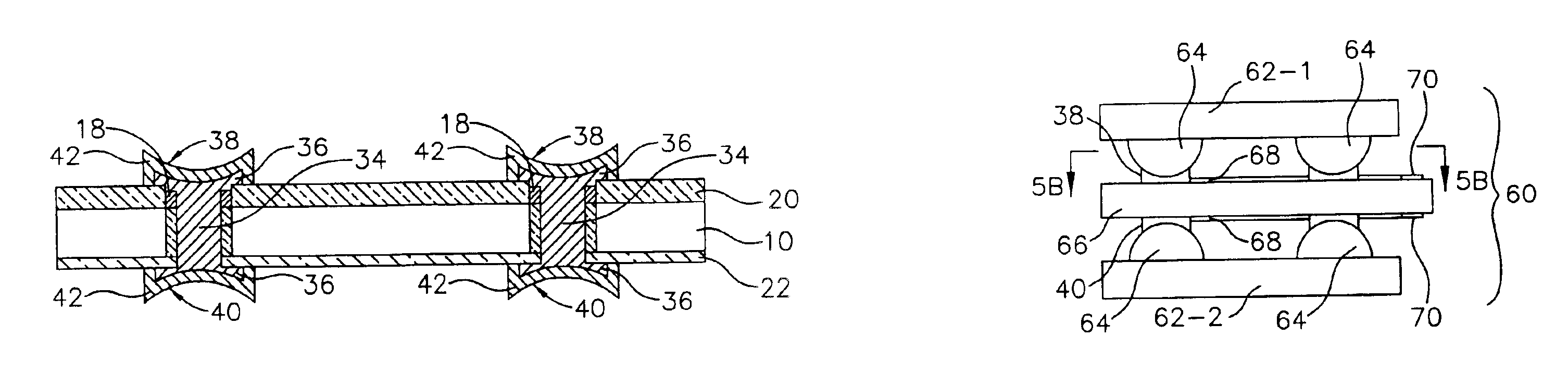
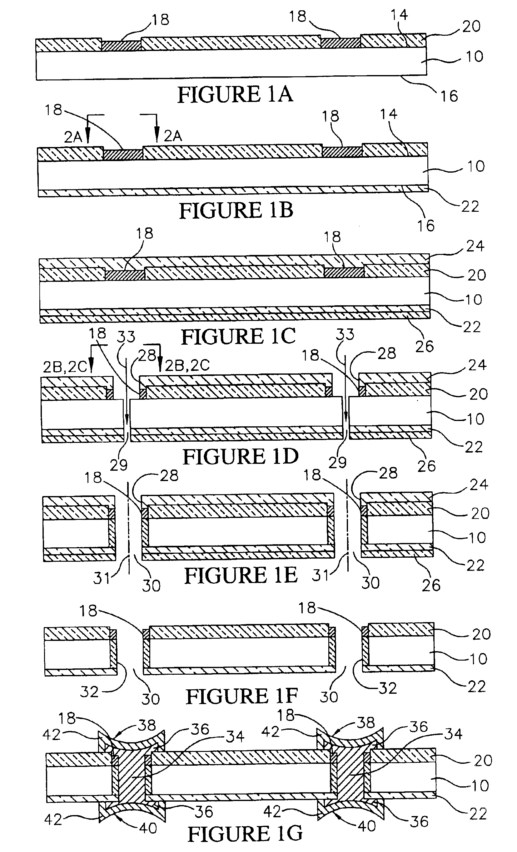
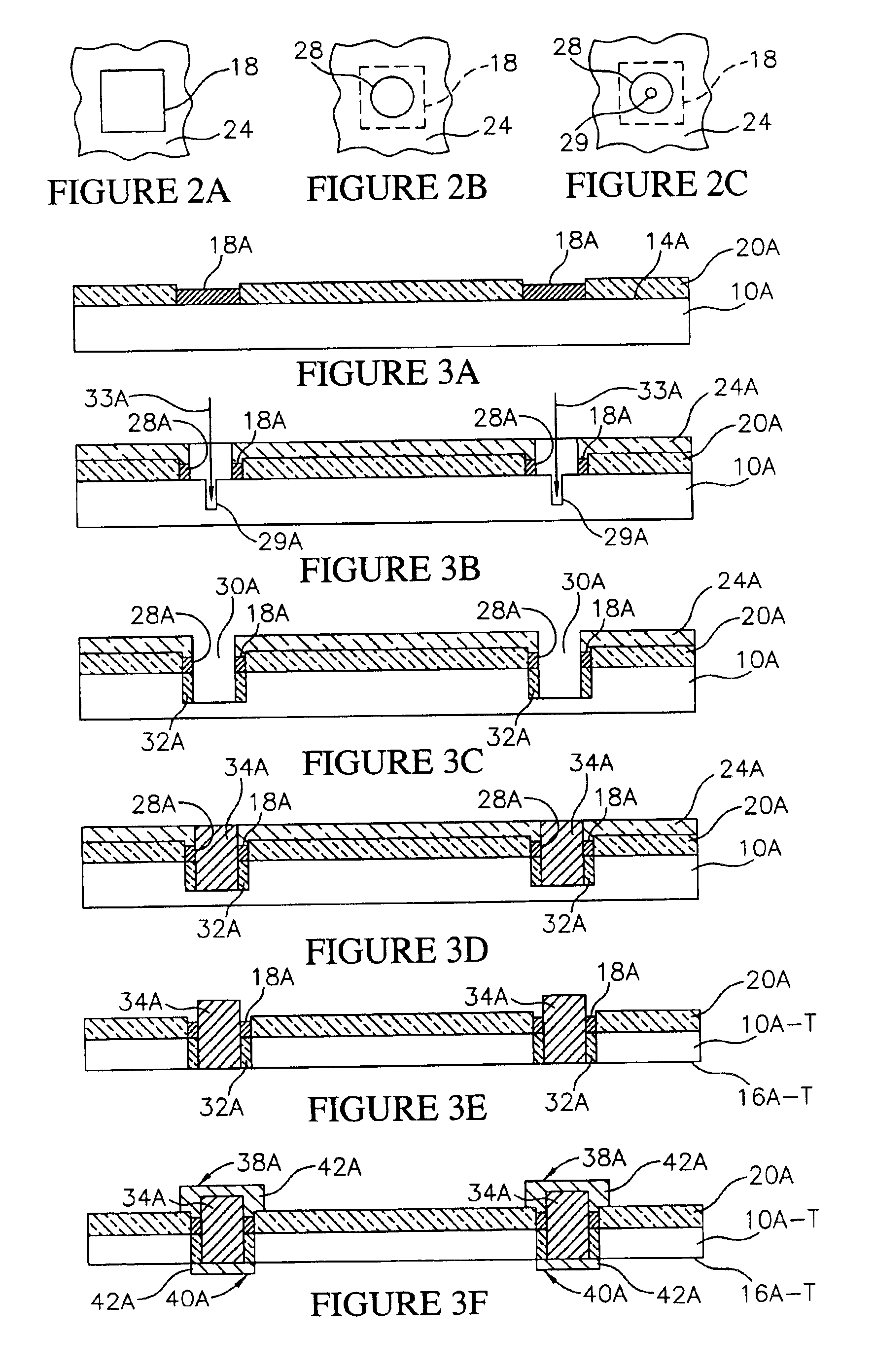
[0033]Referring to FIGS. 1A-1G, a method for fabricating semiconductor components and interconnects in accordance with the invention is illustrated. Initially as shown in FIG. 1A, a substrate 10 is provided. Preferably, the substrate 10...


PUM


Abstract

A method for fabricating semiconductor components and interconnects includes the steps of providing a substrate, such as a semiconductor die, forming external contacts on opposing sides of the substrate by laser drilling vias through the substrate, and forming conductive members in the vias. The conductive members include enlarged terminal portions that are covered with a non-oxidizing metal. The method can be used to fabricate stackable semiconductor packages having integrated circuits in electrical communication with the external contacts. The method can also be used to fabricate interconnects for electrically engaging packages, dice and wafers for testing or for constructing electronic assemblies.

Description

CROSS REFERENCE TO RELATED APPLICATIONS[0001]This application is a division of Ser. No. 10 / 035,355, filed Jan. 4, 2002, U.S. Pat. No. 6,620,731 B1, which is a continuation-in-part of Ser. No. 09 / 961,646, filed Sep. 25, 2001, now U.S. Pat. No. 6,833,613, which is a division of Ser. No. 09 / 385,606, filed Aug. 30, 1999, U.S. Pat. No. 6,294,837, which is a division of Ser. No. 08 / 993,965, filed Dec. 18, 1997, U.S. Pat. No. 6,107,109.FIELD OF THE INVENTION[0002]This invention relates generally to semiconductor manufacture, and specifically to a method for fabricating semiconductor components and interconnects with contacts on opposing sides.BACKGROUND OF THE INVENTION[0003]Semiconductor components include external contacts that allow electrical connections to be made from the outside to the integrated circuits contained on the components. A semiconductor die, for example, includes patterns of bond pads formed on the face of the die. Semiconductor packages, such as chip scale packages, al...

Claims


Application Information

Patent Timeline
Patent Type & Authority Patents(United States)
IPC IPC(8): H01L21/48H01L21/02H01L23/538H01L21/60H01L23/52H01L23/13H01L21/70H01L23/12H01L21/768H01L23/498H01L23/48H01L25/10H05K1/11H05K3/00H05K1/03
CPCH01L21/486H01L21/76898H01L23/13H01L23/481H01L23/49827H01L23/5389H01L24/16H01L24/75H01L24/81H01L25/0657H01L25/105H01L25/50H05K1/112H01L21/6835H01L2224/13099H01L2224/13111H01L2224/13144H01L2224/13147H01L2224/16225H01L2224/73204H01L2224/75H01L2224/81801H01L2224/82039H01L2225/06513H01L2225/06541H01L2924/01004H01L2924/01013H01L2924/0102H01L2924/01022H01L2924/01027H01L2924/01029H01L2924/01032H01L2924/01039H01L2924/01042H01L2924/01046H01L2924/01047H01L2924/01073H01L2924/01074H01L2924/01077H01L2924/01078H01L2924/01079H01L2924/09701H01L2924/14H01L2924/15311H05K1/0306H05K3/0029H05K3/0032H05K2201/09472H05K2201/0959H05K2201/09827H05K2201/09845H05K2201/10674H05K2201/10734H01L2924/01006H01L2924/01033H01L2924/01075H01L2924/01087H01L2924/014H01L2225/1058H01L2225/1005H01L2224/16235H01L2924/00H01L2924/12042H01L2224/0557H01L2224/05573H01L2224/05569H01L2224/05009H01L2224/05568H01L2224/05001H01L2224/0615
Inventor FARNWORTH, WARREN M.WOOD, ALAN G.HEMBREE, DAVID R.
Owner ROUND ROCK RES LLC
Why Eureka
Try Eureka