Wafer polishing method and wafer polishing apparatus in semiconductor fabrication equipment

Inactive Publication Date: 2005-06-14
LONGITUDE SEMICON S A R L
View PDF8 Cites 31 Cited by
  • Summary
  • Abstract
  • Description
  • Claims
  • Application Information

AI Technical Summary

Benefits of technology

[0011]It is an object of the present invention to provide a wafer polishing apparatus and a method capable of polishing a wafer at a stable polishing quantity by accurately detecting the surface state of an

Problems solved by technology

Because abrasion or loading occurs on the surface of the abrasive pad due to polishing, the abrasive pad is damaged and thereby, the polishing efficiency is deteriorated.
In the case of this method, however, because it is necessary to regularly polish and examine the dummy wafer whenever the polishing is executed in predetermined times, lots of time and labor are necessary and this causes the wafer fabrication cost to increase.
However, as described above, the method for detecting the friction force between a conditioner and an abrasive pad in accordance with the deflection value of a balanced spring has a problem that the sensitivity is too low.
This is because a structure is used in which a balanced spring for being detected its deflection value is not easily deflected since it rotates together with a detection section and moreover, a pressure is applied.
However, when increasing the

Method used


Image

  • Wafer polishing method and wafer polishing apparatus in semiconductor fabrication equipment
  • Wafer polishing method and wafer polishing apparatus in semiconductor fabrication equipment
  • Wafer polishing method and wafer polishing apparatus in semiconductor fabrication equipment

Examples


Example

First Embodiment

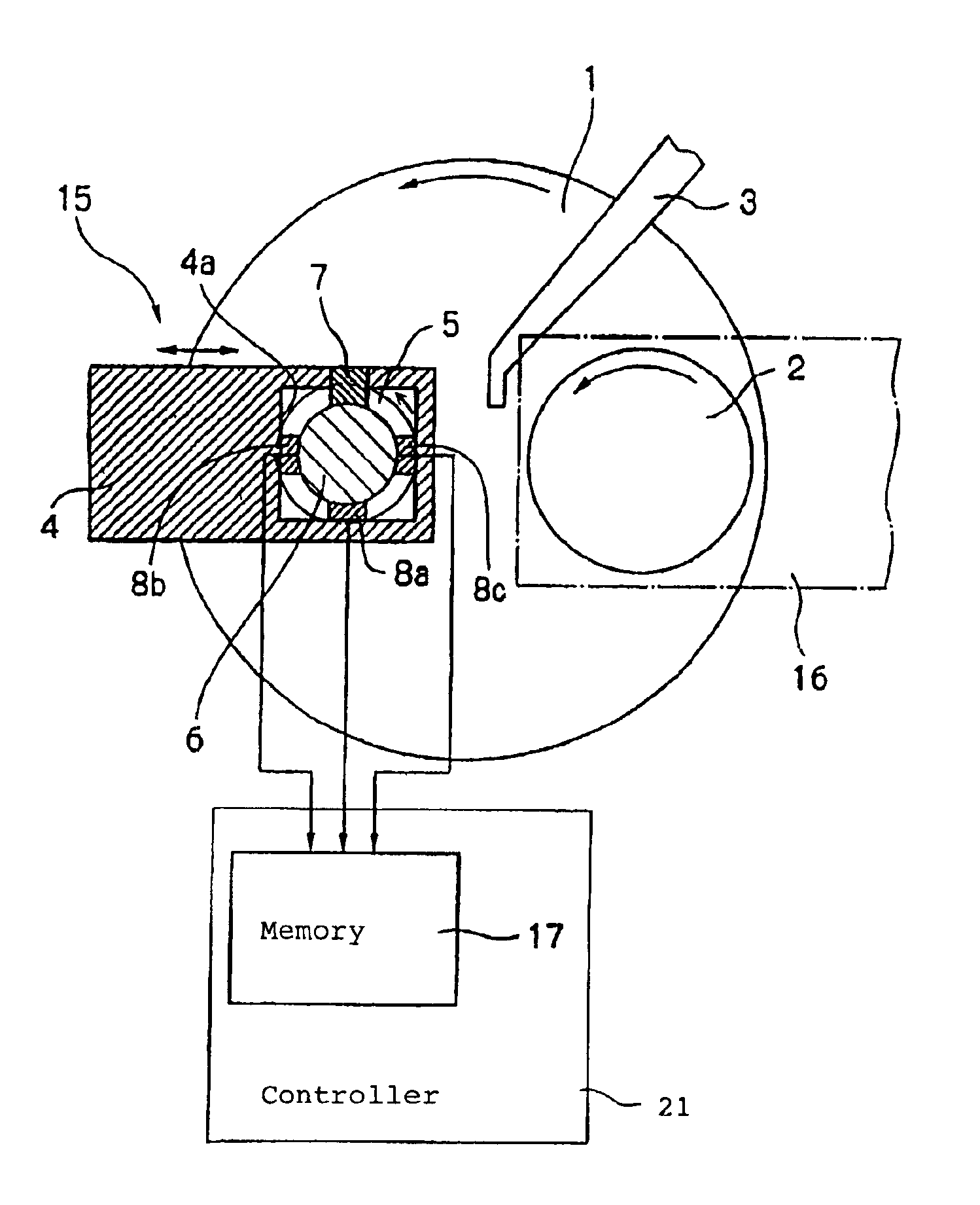
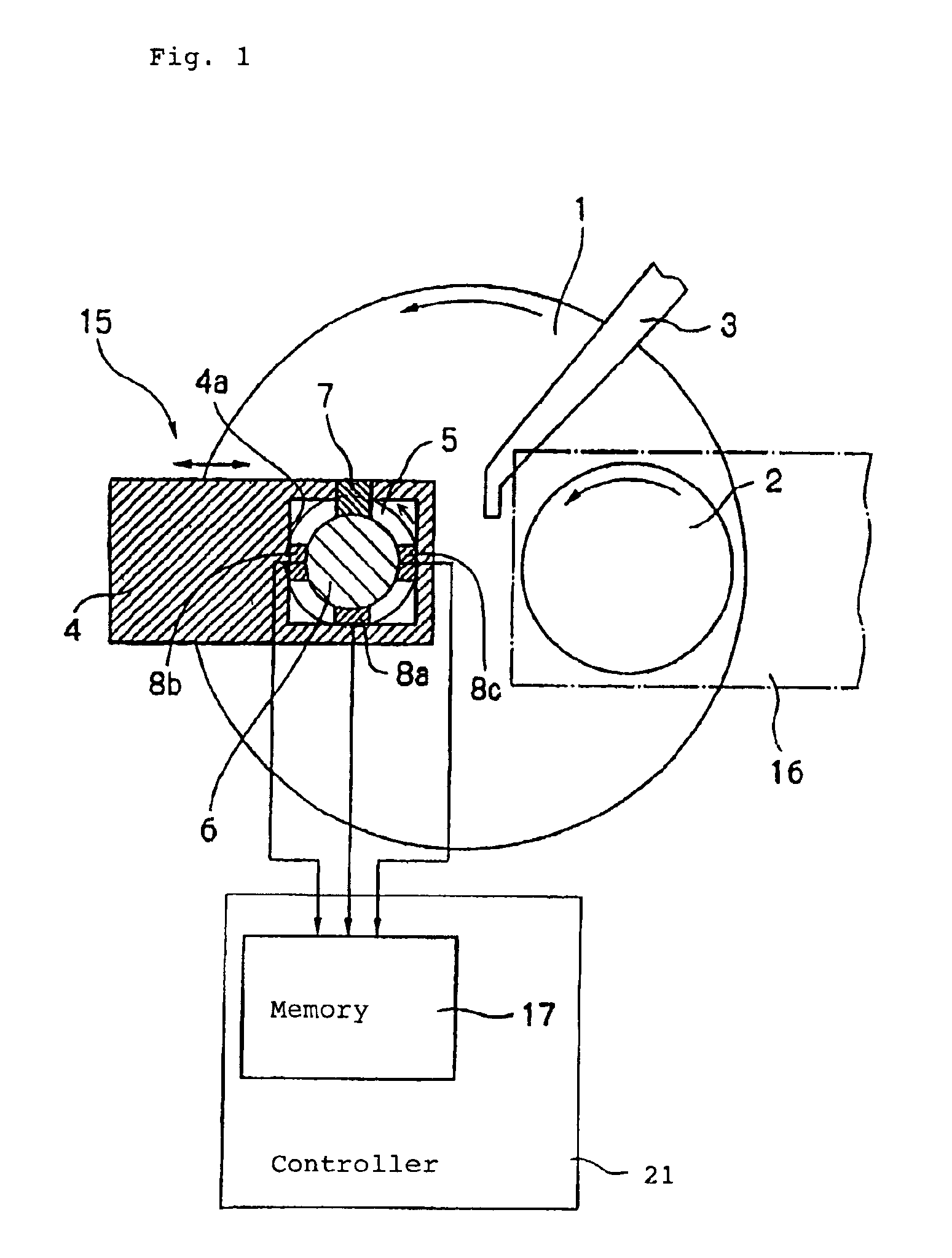
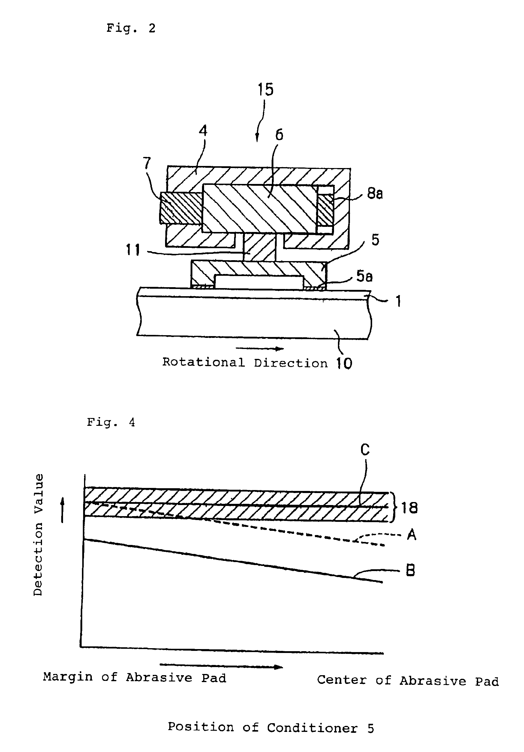
[0028]The wafer polishing apparatus of the first embodiment of the present invention will be described below referring to FIGS. 1 and 2. FIG. 1 is a top view of the wafer polishing apparatus of the first embodiment. The wafer polishing apparatus has a circular platen 10, an abrasive pad 1 attached onto the platen 10, a wafer holding head 16 provided so as to face one part of the platen 10, a conditioning mechanism 15 provided so as to face the other part of the platen 10, and a nozzle 3. The abrasive pad 1 is made of elastic polyurethane or the like. The wafer holding head 16 holds the back surface of a wafer 2. The nozzle 3 supplies deionized water or slurry between the abrasive pad 1 and wafer 2. The conditioning mechanism 15 has a cantilever-shaped arm 4, a conditioner driving unit 6, a conditioner 5 held by the conditioner driving unit 6, a fixing jig 7, and three pressure detectors 8a to 8c. The arm 4 is able to relatively move against the platen 10. A diamond 5...

Example

Second Embodiment

[0043]Then, a second embodiment of the present invention will be described below referring to FIG. 5. A portion same as that of the first embodiment is provided with the same reference number and its description is omitted.

[0044]A conditioning mechanism 19 of this embodiment is constituted so that a rotating shaft 11 for connecting a conditioner 5 with a conditioner driving unit 6 is supported by an upper rotation bearing 12 and a lower rotation bearing 13 in order to further improve the detection sensitivity. The upper rotation bearing 12 is fixed to the conditioner driving unit 6 and an arm 4 by screws. The lower rotation bearing 13 is connected to the arm 4 through a piezoelectric element serving as a pressure detector 20 by a lower rotation bearing fixing plate 14. A force working on the conditioner 5 under conditioning is obtained by detecting the deflection of the rotating shaft 11 by the pressure detector 20 between the lower rotation bearing fixing plate 14 ...


PUM

PropertyMeasurementUnit
Forceaaaaaaaaaa

Abstract

When honing an abrasive pad for polishing a wafer by rotating while closely contacting the wafer by bringing a conditioner into contact with the abrasive pad, forces applied from the abrasive pad to the conditioner are detected by a plurality of pressure detectors through a conditioner driving unit for holding the conditioner. The pressure detectors are respectively able to detect forces in two directions such as rotational direction and radial direction. A memory stores correlations between detection values and wafer polishing quantities under various conditioning terms. Therefore, it is determined whether the detection values are kept within acceptable limits stored in the memory. When the values are out of the acceptable limits, a controller controls the values so that they fall within the acceptable limits by properly changing conditioning terms.

Description

BACKGROUND OF THE INVENTION[0001]1. Field of the Invention[0002]The present invention relates to a wafer polishing method and apparatus in semiconductor fabrication equipment, and more particularly to a wafer polishing apparatus and method capable of sufficiently controlling the polishing quantity of a wafer serving as a semiconductor substrate and continuously polishing the wafer at a stable polishing quantity.[0003]2. Description of the Related Art[0004]Various micro-fabrication techniques have been researched and developed in order to improve integration degree and functions of an LSI. Attention has been paid to a chemical mechanical polishing (hereinafter referred to as “CMP”) technique which is one of the micro-fabrication techniques. The CMP is a polishing technique with a combination of a chemical action between an abrasive (slurry) and an object to be polished (wafer), and a mechanical action by abrasive grains in the slurry. This is technique useful in flattening an insulat...

Claims


Application Information

Patent Timeline
IPC IPC(8): B24B37/04B24B53/007H01L21/02H01L21/306B24B53/017B24B53/02H01L21/304
CPCB24B53/017H01L21/30625
Inventor SAKUMA, NORIYUKITSUNENARI, KINJI
Owner LONGITUDE SEMICON S A R L
Why Eureka
Try Eureka