Method of forming interconnect structure with low dielectric constant

Inactive Publication Date: 2005-06-14
UNITED MICROELECTRONICS CORP
View PDF6 Cites 15 Cited by
  • Summary
  • Abstract
  • Description
  • Claims
  • Application Information

AI Technical Summary

Benefits of technology

[0010]It is another object of the present invention to provide a method for forming an interconnect structure. The interconnect structure can be with characteristics of low dielectric constant and enhanced mechanical strength.
[0011]It is yet other object of t

Problems solved by technology

On the other hand, considerable attention has focused on the replacement of silicon dioxide with new materials, particular material having lower dielectric constants, since both capacity delays and power consumption depend on the dielectric constant of insulator.
However, the spin on dielectric (SOD

Method used


Image

  • Method of forming interconnect structure with low dielectric constant
  • Method of forming interconnect structure with low dielectric constant
  • Method of forming interconnect structure with low dielectric constant

Examples


Example

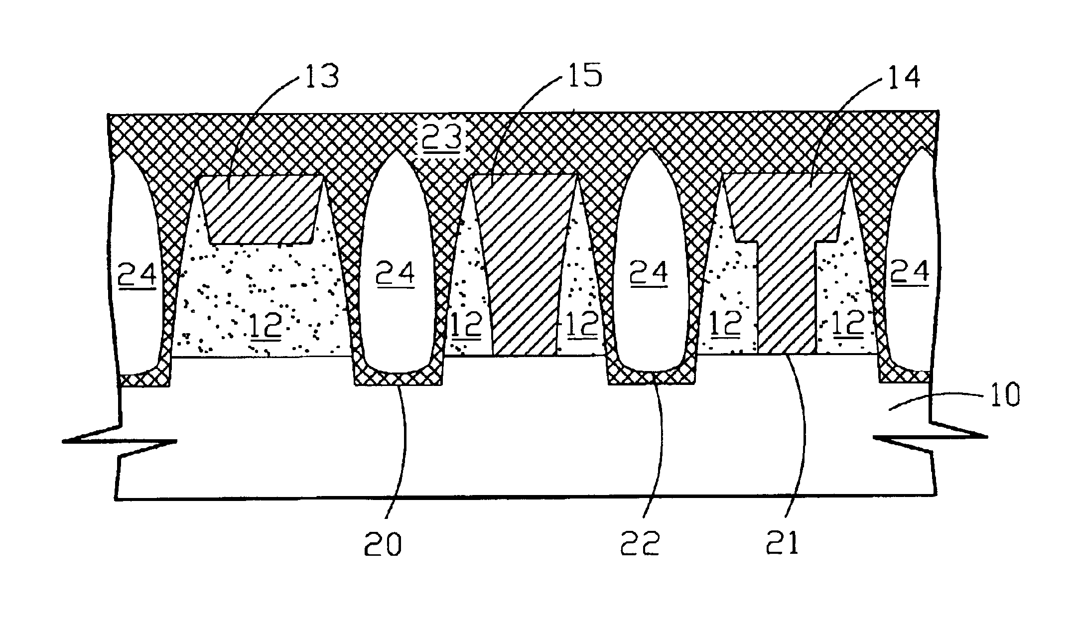
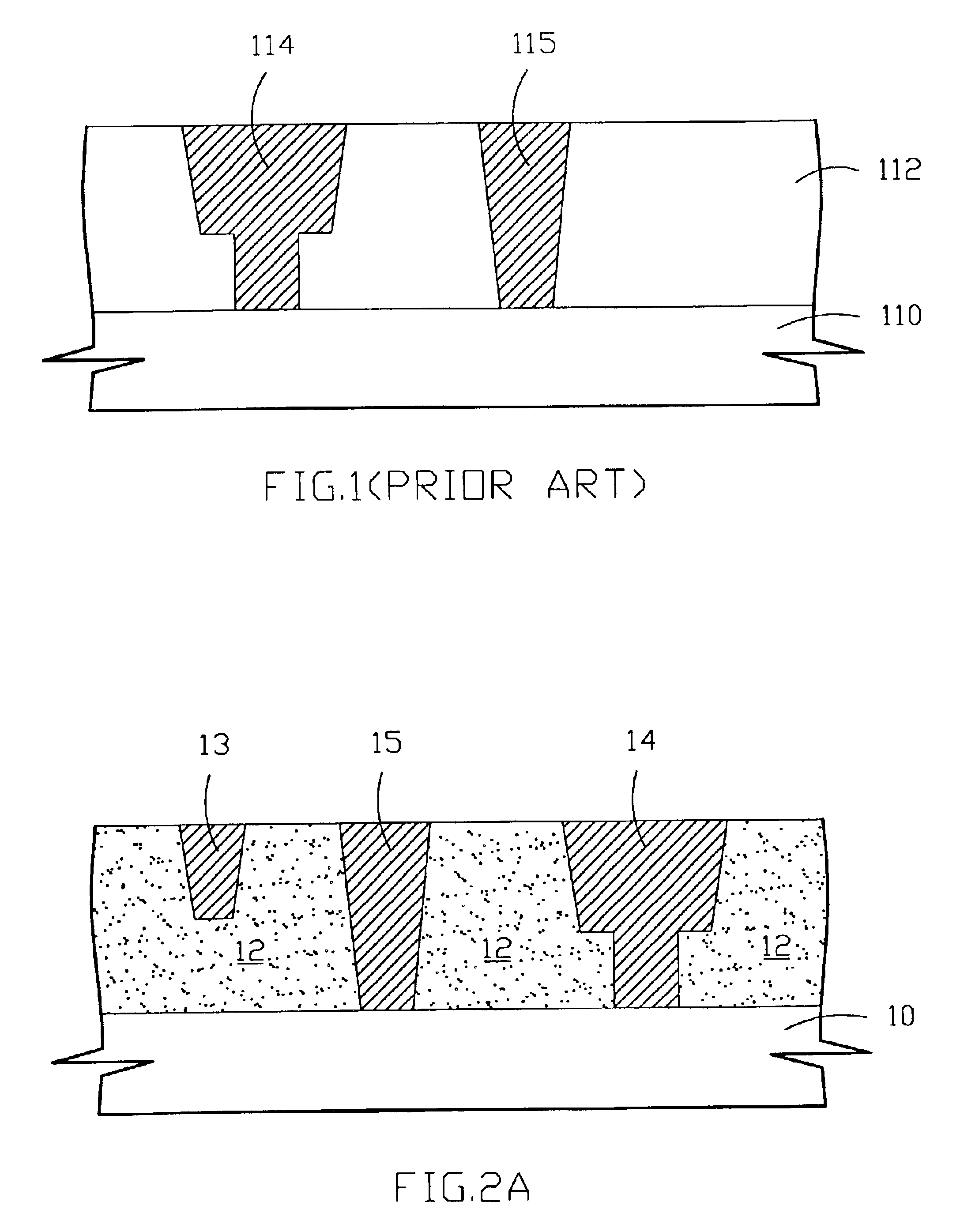
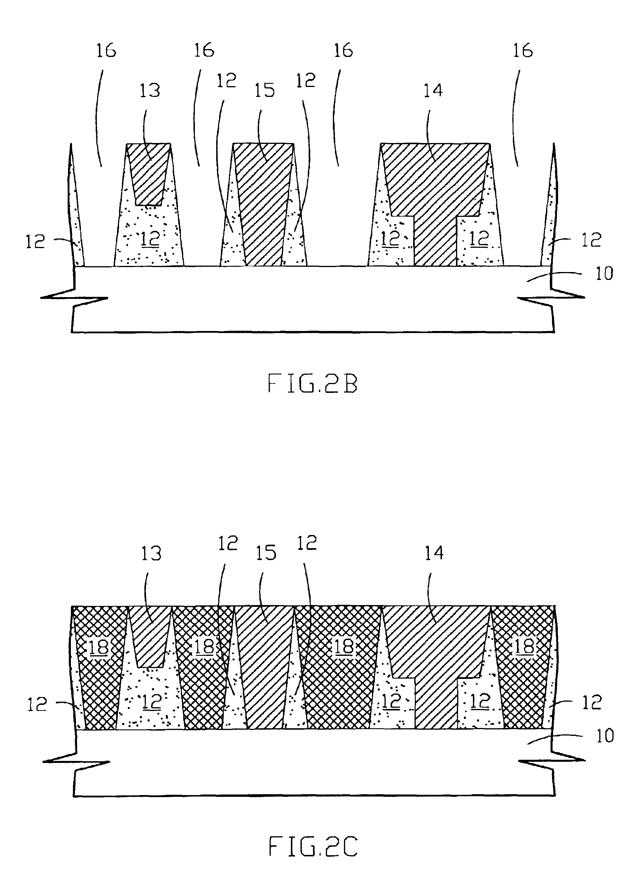
[0017]The semiconductor devices of the present invention are applicable to a board range of semiconductor devices and can be fabricated from a variety of semiconductor materials. While the invention is described in terms of a single preferred embodiment, those skilled in the art will recognize that many steps described below can be altered without departing from the spirit and scope of the invention.

[0018]Furthermore, there is shown a representative portion of a semiconductor structure of the present invention in enlarged, cross-sections of the two dimensional views at several stages of fabrication. The drawings are not necessarily to scale, as the thickness of the various layers are shown for clarify of illustration and should not be interpreted in a limiting sense. Accordingly, these regions will have dimensions, including length, width and depth, when fabricated in an actual device.

[0019]In the present invention, a method is for forming low dielectric constant inter-metal dielect...


PUM


Abstract

The present invention provides a method for forming low dielectric constant inter-metal dielectric layer. The method includes providing a semiconductor substrate and forming a first dielectric layer on the semiconductor substrate. Conductor structures are formed in the first dielectric layer. The partial first dielectric layer is removed by using the conductor structures as etching mask. A second dielectric layer is formed between the conductor structures, which has a dielectric constant smaller than the first dielectric layer. The second dielectric layer also alternatively has air voids contained therein to reduce dielectric constant.

Description

[0001]This application is a continuation-in-part of original U.S. patent application Ser. No. 09 / 840,715 filed on Apr. 24, 2001 now abandoned.BACKGROUND OF THE INVENTION[0002]1. Field of the Invention[0003]The invention relates to a method for forming interconnect structures, and more particularly to a method for forming interconnect structures with a low dielectric constant.[0004]2. Description of the Prior Art[0005]It is the nature of semiconductor physics that as the feature sizes are scaled down, the performance of internal devices in integrated circuits improves in a compounded fashion. That is, the device speed as well as the functional capability improves. The overall circuit speed, however, becomes more dependent upon the propagation speed of the signals along interconnects that connect the various devices together. With the advent of very and ultra large scale integration (VLSI and ULSI) circuits, it has therefore become even more important that the metal conductors that fo...

Claims


Application Information

Patent Timeline
IPC IPC(8): H01L23/52H01L23/522H01L21/70H01L21/768H01L23/532H01L21/02H01L21/318H01L21/316
CPCH01L23/5329H01L21/76801H01L23/5222H01L21/31612H01L21/31625H01L21/31629H01L21/318H01L2924/0002H01L2924/00
Inventor YANG, MING-SHENGLIU, CHIH-CHIEN
Owner UNITED MICROELECTRONICS CORP
Why Eureka
Try Eureka